Quick Navigation
- Report Overview
- Key Statistics
- Key Takeaways
- Regional Analysis
- By Component
- By Wafer Size
- By Automation Level
- By Application
- Key Market Segments
- Driving Factors
- Restraining Factors
- Growth Opportunities
- Challenging Factors
- Growth Factors
- Emerging Trends
- Business Benefits
- Key Players Analysis
- Recent Developments
- Report Scope
Report Overview
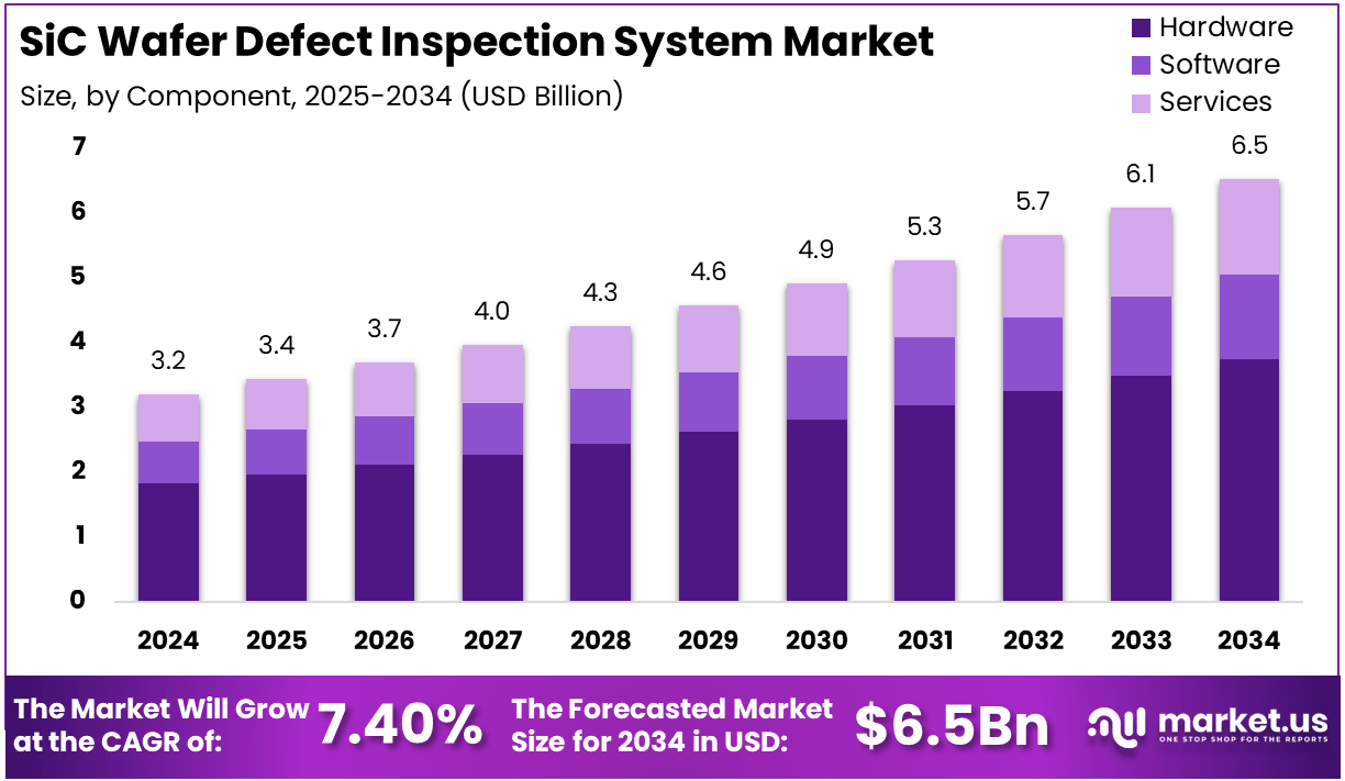
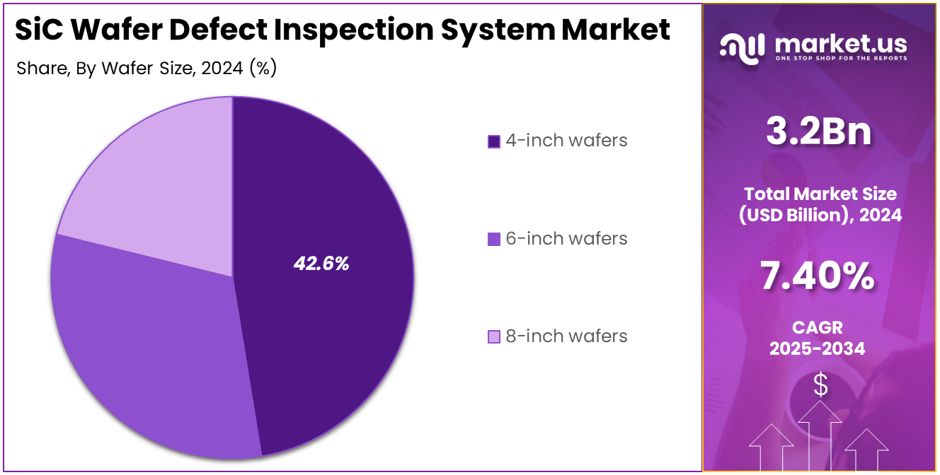
The Global SiC Wafer Defect Inspection System Market size is expected to be worth around USD 6.5 Billion By 2034, from USD 3.2 Billion in 2024, growing at a CAGR of 7.40% during the forecast period from 2025 to 2034.
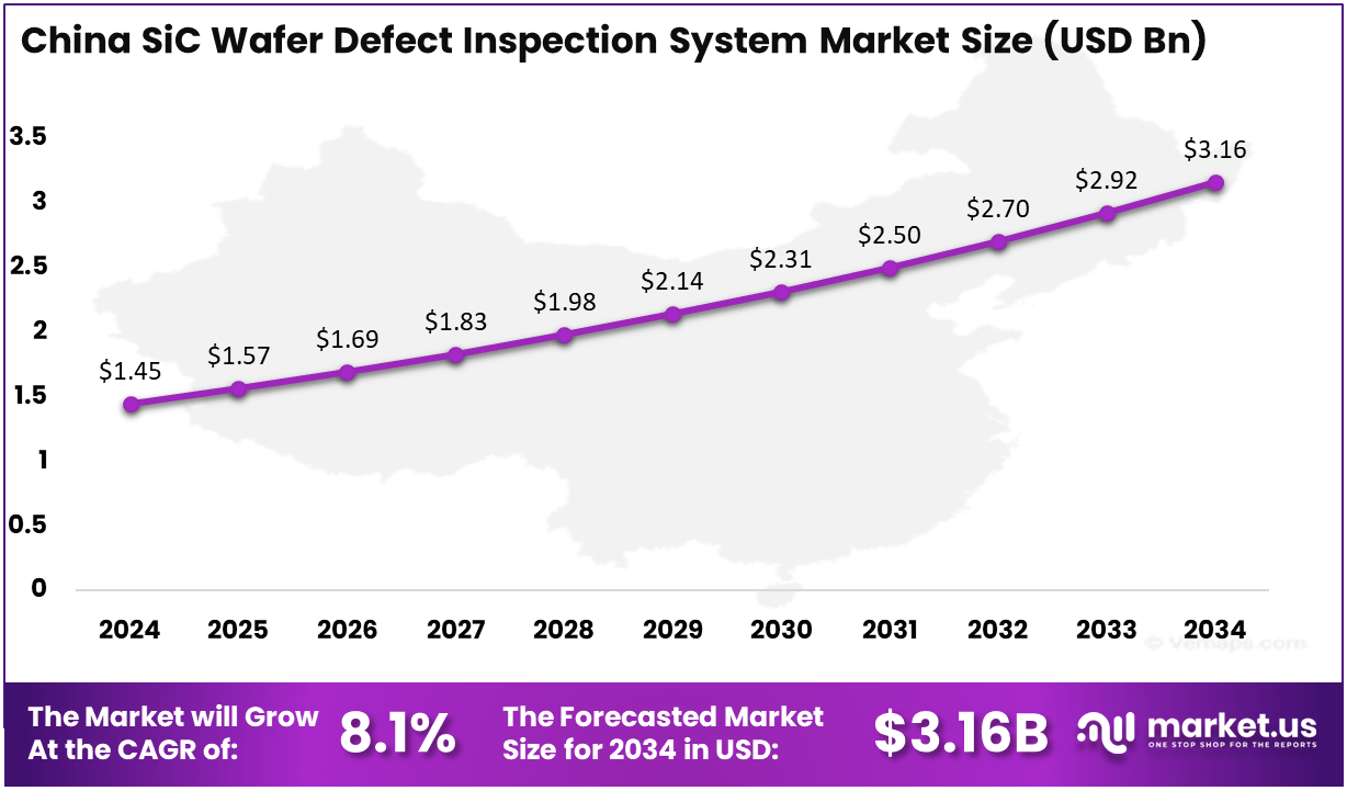
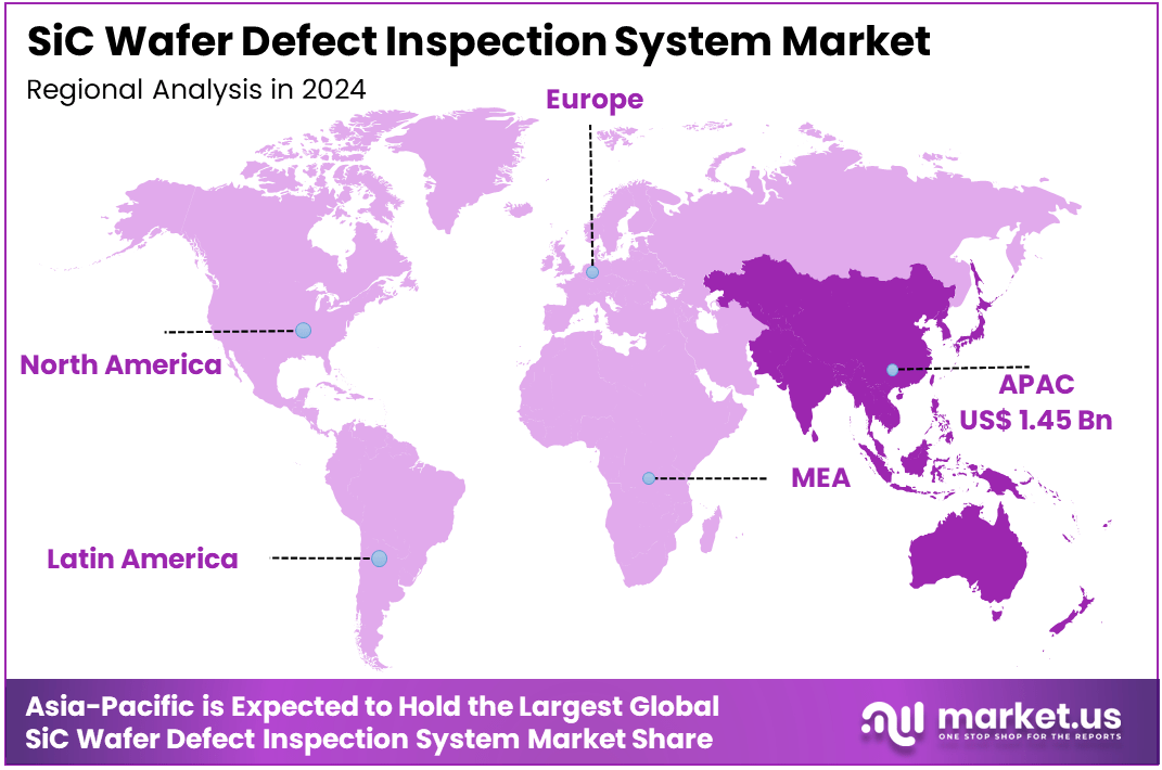
In 2024, Asia-Pacific held a dominant market position, capturing more than a 42.4% share, holding USD 1.45 Billion in revenue. Further, In Asia-Pacific, China dominates the market size by USD 0.83 Billion holding the strong position steadily with a CAGR of 8.1%.
A Silicon Carbide (SiC) wafer defect inspection system is a high-tech tool used in the manufacturing process of SiC wafers, which are a key component in power electronics, particularly in electric vehicles (EVs), renewable energy, and telecommunications.
SiC wafers are known for their ability to withstand higher temperatures, voltages, and frequencies compared to traditional silicon wafers. The defect inspection system helps identify minute defects and impurities on the wafer’s surface during production, ensuring that only high-quality wafers make it to the next stages of semiconductor manufacturing.
These inspection systems utilize advanced imaging, laser, and sometimes even machine learning-based methods to identify flaws that could lead to failures in the final product. The accuracy and speed of these systems are crucial in the high-stakes, high-precision world of semiconductor fabrication.
Key Statistics
Material: Silicon Carbide (SiC)
- SiC is a semiconductor material known for its high thermal conductivity, high electric field breakdown strength, and high-temperature stability. This makes it ideal for power electronics, especially in applications like electric vehicles and renewable energy systems.
Function: Inspection of defects on SiC wafers
- The defect inspection system ensures that the wafers produced are free from defects that could affect the performance of the final semiconductor devices. This is critical for maintaining yield and reliability in production.
User Base:
- The primary users of SiC wafer defect inspection systems are semiconductor manufacturers who specialize in power devices. These manufacturers are increasingly focusing on SiC technology due to its advantages over traditional silicon in high-power applications.
Usage:
- Final Visual Inspection: Ensures that wafers meet quality standards before they are used in device fabrication.
- Inspection After Lapping, Grinding, and Polishing: Detects any defects introduced during these mechanical processes, which are critical for achieving the desired surface quality.
Wafer Sizes Supported:
- 200 mm (8-inch): A common size used in many semiconductor fabs.
- 300 mm (12-inch): Larger wafers that provide higher throughput and efficiency in manufacturing.
Inspection Time:
- The typical throughput of the inspection system ranges from 30 to 90 seconds per wafer, depending on the complexity of the inspection process required. Faster inspection times contribute to overall manufacturing efficiency.
Load Port Capacity:
- The system can accommodate a minimum of 2 cassettes and a maximum of 10 cassettes, allowing for flexible loading and unloading of wafers. This capacity supports both 6-inch and 8-inch wafers, making it versatile for various production needs.
Inspection Sensitivity:
- Surface defects as small as 0.3 µm, ensuring high-quality surfaces.
- Edge defects ranging from 1 to 10 µm, are critical for maintaining edge integrity during device fabrication.
- Internal defects also range from 1 to 10 µm, which can significantly impact device performance.
The SiC wafer defect inspection system market is experiencing rapid growth, driven primarily by the increasing demand for SiC wafers across various high-growth industries like electric vehicles (EVs), renewable energy, and telecommunications.
As the adoption of EVs grows, and the push for energy-efficient solutions intensifies, the need for SiC wafers—due to their superior properties over traditional silicon—has surged. As a result, the demand for defect inspection systems, which ensure the quality and performance of these wafers, is also rising.
The market is also being driven by advancements in semiconductor technology, pushing the need for more precise and reliable inspection methods. Companies involved in the development of defect inspection systems are increasingly focused on improving the speed, accuracy, and efficiency of these systems, further expanding the market.
Several factors are driving the growth of the SiC wafer defect inspection system market. First and foremost, the demand for SiC-based components in electric vehicles is surging, owing to their ability to handle high power densities and enable better energy efficiency. As the automotive industry accelerates its transition to electric vehicles, SiC wafers have become indispensable in the production of power devices such as inverters and converters.
Additionally, the increasing need for more efficient and robust power electronics in industries like renewable energy and telecommunication systems is boosting the demand for SiC wafers and, in turn, the inspection systems required to ensure their quality. Technological advancements in automation and machine learning are also enabling defect inspection systems to perform with higher precision, further driving market growth.
The market demand for SiC wafer defect inspection systems is being fueled by the growing investment in industries that heavily rely on SiC-based components, such as the electric vehicle market. As the global push for carbon neutrality and renewable energy solutions intensifies, more manufacturers are looking to SiC as a critical material for power electronics.
The SiC wafer defect inspection system market is poised for significant opportunities. As the adoption of SiC wafers continues to grow in industries beyond automotive—such as renewable energy, aerospace, and industrial power systems—the market for inspection systems will expand accordingly.
Technological advancements are continuously shaping the SiC wafer defect inspection system market. One of the most notable developments is the use of artificial intelligence and machine learning to enhance defect detection accuracy. AI-powered systems can analyze large volumes of data in real-time, identifying even the smallest defects that may go unnoticed by traditional methods.
Key Takeaways
- Market Value Growth: The SiC Wafer Defect Inspection System market is projected to grow from USD 3.2 billion in 2024 to USD 6.5 billion in 2034, at a CAGR of 7.40%.
- Component Breakdown: Hardware accounts for 57.4% of the market share, reflecting its dominance in the SiC wafer defect inspection system.
- Wafer Size Distribution: 4-inch wafers represent 42.6% of the market, highlighting their significant presence in the industry.
- Automation Level: Fully Automated Systems are expected to hold 40.4% of the market, indicating a trend towards higher automation in defect inspection.
- Application Focus: The Power Electronics sector leads with 54.7% of the market share, driven by the increasing demand for SiC wafers in high-performance power devices.
- Regional Distribution: Asia-Pacific holds 45.6% of the market share, underscoring its dominance in the SiC wafer defect inspection system market.
- China’s Market Size: China is projected to reach USD 1.45 billion, growing at a CAGR of 8.1%, indicating a rapidly expanding market within the region.
Regional Analysis
China Wafer Defect Inspection System Market Size
China, in particular, is a significant contributor, with the market expected to grow at a CAGR of 8.1%, and revenue at USD 3.16 Billion making it one of the fastest-growing markets for SiC wafer defect inspection systems. The increasing investments in clean energy and electric vehicles in China are expected to sustain this growth, making the region an essential player in the global SiC wafer defect inspection landscape.
In conclusion, Asia-Pacific’s dominance is driven by its robust manufacturing capabilities, technological advancements, and the rapidly expanding industries relying on SiC-based components. The region’s increasing focus on high-quality production processes, combined with the rise in demand for electric vehicles and renewable energy solutions, ensures that Asia-Pacific will continue to lead the SiC Wafer Defect Inspection System market for the foreseeable future.
Asia Pacific SiC Wafer Defect Inspection System Market
In 2024, Asia-Pacific held a dominant market position, capturing more than a 42.4% share of the SiC Wafer Defect Inspection System market, with USD 1.45 billion in revenue. The region’s leadership can be attributed to its strong manufacturing base, particularly in countries like China, Japan, and South Korea, which are major producers of SiC wafers.
Asia-Pacific is at the forefront of industries that heavily rely on SiC-based components, such as power electronics, automotive (especially electric vehicles), and renewable energy sectors. The rapid expansion of electric vehicle production and the growing need for energy-efficient power devices have significantly contributed to the demand for SiC wafers and, by extension, for defect inspection systems.
Additionally, Asia-Pacific is home to some of the largest semiconductor manufacturers, which continue to invest in advanced technologies for wafer production. The growing emphasis on automation, precision manufacturing, and the integration of AI-based inspection systems has further strengthened the region’s market position. With a booming demand for SiC-based solutions in both automotive and power electronics, Asia-Pacific remains a hub for innovation and production, maintaining its dominance in the SiC Wafer Defect Inspection System market.
By Component
In 2024, the Hardware segment held a dominant market position, capturing more than a 57.4% share of the SiC Wafer Defect Inspection System market. This dominance is primarily driven by the increasing demand for high-precision and reliable defect detection in the manufacturing of SiC wafers, which are critical components in power electronics.
Hardware components such as high-resolution imaging systems, sensors, and laser-based technologies are integral to the inspection process, enabling the identification of minute defects at various stages of wafer production. The growth of industries such as electric vehicles (EVs), renewable energy, and telecommunications, all of which require SiC wafers, has further fueled the demand for these hardware solutions.
Additionally, the rapid advancement in hardware technologies—particularly in terms of speed, accuracy, and automation—has made these systems more efficient and cost-effective, leading to increased adoption. As a result, hardware continues to be the driving force in the SiC Wafer Defect Inspection System market, establishing its leading position.
By Wafer Size
In 2024, the 4-inch wafers segment held a dominant market position, capturing more than a 42.6% share of the SiC Wafer Defect Inspection System market. This segment’s leadership can be attributed to the widespread use of 4-inch wafers in power electronics applications, particularly in the automotive and renewable energy sectors.
The 4-inch wafer size is considered ideal for many SiC-based devices, including power semiconductors, due to its balance between performance, cost, and production scalability. As industries such as electric vehicles (EVs) and energy-efficient systems continue to grow, the demand for high-quality SiC wafers has surged, further strengthening the role of 4-inch wafers in manufacturing.
Additionally, the cost-effectiveness of producing 4-inch wafers, compared to larger wafer sizes, makes them a preferred choice for companies looking to optimize both performance and yield. This combination of factors—demand in key industries, production efficiency, and cost-effectiveness—has allowed the 4-inch wafer segment to maintain its leading position in the SiC Wafer Defect Inspection System market.
By Automation Level
In 2024, the Fully Automated Systems segment held a dominant market position, capturing more than a 40.4% share of the SiC Wafer Defect Inspection System market. The growth of this segment is primarily driven by the increasing demand for faster, more efficient, and precise defect detection in high-volume SiC wafer production.
Fully automated systems offer significant advantages over manual and semi-automated systems, including higher throughput, reduced human error, and the ability to operate continuously without interruptions. This automation not only enhances the speed of defect detection but also improves the consistency and accuracy of inspections, which are crucial for maintaining the high quality of SiC wafers used in critical applications like power electronics and electric vehicles.
As industries push for higher production efficiency and lower costs, the transition toward fully automated inspection systems has become a natural progression. The increasing focus on optimizing manufacturing processes and minimizing defects has cemented the position of fully automated systems as the leading choice in the market.
By Application
In 2024, the Power Electronics segment held a dominant market position, capturing more than a 54.7% share of the SiC Wafer Defect Inspection System market. The dominance of this segment can be attributed to the growing demand for Silicon Carbide (SiC) wafers in power electronics, particularly in high-performance devices such as inverters, converters, and power management systems.
SiC wafers are preferred in power electronics for their ability to handle high temperatures, voltages, and frequencies, making them essential in applications like electric vehicles, renewable energy systems, and industrial equipment. As industries focus on improving energy efficiency and reducing carbon footprints, the need for high-quality SiC-based power electronics continues to rise.
The increasing adoption of electric vehicles and renewable energy technologies further amplifies this demand. Consequently, the inspection systems for SiC wafers used in power electronics play a vital role in ensuring the reliability and performance of these critical devices. This has positioned the power electronics segment as the largest and fastest-growing application within the SiC wafer defect inspection market.
Key Market Segments
By Component
- Hardware
- Software
- Services
By Wafer Size
- 4-inch wafers
- 6-inch wafers
- 8-inch wafers
By Automation Level
- Manual Systems
- Semi-automated Systems
- Fully Automated Systems
By Application
- Power Electronics
- Wireless Communication
- Automotive
- Renewable Energy
- Others
Driving Factors
Increasing Demand for SiC-based Semiconductor Devices
The escalating adoption of Silicon Carbide (SiC) in power electronics is a significant driver for the SiC Wafer Defect Inspection System market. SiC’s superior properties, such as high thermal conductivity, wide bandgap, and high voltage tolerance, make it ideal for high-performance applications like electric vehicles (EVs), renewable energy systems, and industrial power devices.
As industries strive for greater energy efficiency and performance, the demand for SiC-based devices has surged, necessitating advanced inspection systems to ensure the quality and reliability of SiC wafers used in these applications.
In the automotive sector, particularly with the rise of EVs, SiC components are essential for efficient power conversion and energy management. Similarly, the renewable energy industry relies on SiC-based devices for efficient power conversion in solar inverters and wind turbines.
Restraining Factors
High Initial Investment Costs
A significant challenge in the SiC Wafer Defect Inspection System market is the substantial initial investment required for advanced inspection equipment. These systems incorporate cutting-edge technologies, such as electron microscopy, laser scanning, and X-ray imaging, which come with high development and manufacturing costs.
For smaller manufacturers or startups with limited budgets, the high upfront costs can be prohibitive, potentially hindering their ability to adopt these essential inspection systems.
Additionally, the maintenance and operational costs associated with these sophisticated systems can further strain financial resources. This financial barrier may lead to a slower adoption rate among smaller players in the market, potentially affecting the overall growth and competitiveness of the industry.
Growth Opportunities
Integration of AI and Machine Learning
The integration of Artificial Intelligence (AI) and Machine Learning (ML) technologies into SiC wafer defect inspection systems presents a significant growth opportunity. AI and ML can enhance the accuracy and efficiency of defect detection by analyzing complex data patterns and identifying subtle anomalies that traditional methods might miss. This advancement can lead to higher production yields and reduced waste, offering a competitive edge to manufacturers.
Furthermore, AI-driven systems can enable predictive maintenance, reducing downtime and extending the lifespan of inspection equipment. The ability to automate defect classification and analysis also streamlines the production process, leading to cost savings and improved product quality.
Challenging Factors
Complexity of SiC Wafer Material
The inherent properties of SiC wafers, such as their hardness and brittleness, pose significant challenges for defect inspection. Detecting sub-surface defects, which are often not visible on the wafer’s surface, requires specialized inspection systems capable of penetrating the wafer material without causing damage. This complexity necessitates the development of advanced inspection technologies tailored specifically for SiC wafers, which can be both time-consuming and costly.
Additionally, the variability in SiC wafer quality and the presence of different types of defects, each affecting device performance differently, complicate the inspection process. Developing inspection systems that can accurately identify and classify these diverse defects is a significant technical challenge, requiring continuous innovation and adaptation to new manufacturing processes and materials.
Growth Factors
Surge in Electric Vehicle (EV) Production
The global shift towards electric vehicles (EVs) is a significant growth factor for the SiC Wafer Defect Inspection System market. SiC wafers are essential in EVs for efficient power conversion and energy management.
As EV production increases, the demand for high-quality SiC wafers and, consequently, advanced inspection systems, is expected to rise. The EV market is projected to grow at a compound annual growth rate (CAGR) of 26% through 2030, indicating a substantial increase in demand for SiC-based components.
Emerging Trends
Integration of Artificial Intelligence (AI) in Inspection Systems
The incorporation of AI and machine learning into SiC wafer defect inspection systems is an emerging trend. AI enhances the accuracy and efficiency of defect detection by analyzing complex data patterns and identifying subtle anomalies that traditional methods might miss.
This advancement can lead to higher production yields and reduced waste, offering a competitive edge to manufacturers. The integration of AI is expected to become a key differentiator in the market, as industries increasingly demand higher precision and efficiency.
Business Benefits
Enhanced Production Efficiency and Yield
Implementing advanced SiC wafer defect inspection systems offers significant business benefits, including improved production efficiency and higher yield rates. By accurately identifying and addressing defects early in the manufacturing process, companies can reduce waste and rework, leading to cost savings.
This efficiency not only lowers operational costs but also enhances product quality, meeting the stringent standards required in industries like power electronics and renewable energy. The adoption of such systems is a strategic move for businesses aiming to maintain competitiveness in the rapidly evolving semiconductor market.
Key Regions and Countries
- North America
- US
- Canada
- Europe
- Germany
- France
- The UK
- Spain
- Italy
- Russia
- Netherlands
- Rest of Europe
- Asia Pacific
- China
- Japan
- South Korea
- India
- Australia
- Singapore
- Thailand
- Vietnam
- Rest of APAC
- Latin America
- Brazil
- Mexico
- Rest of Latin America
- Middle East & Africa
- South Africa
- Saudi Arabia
- UAE
- Rest of MEA
Key Players Analysis
KLA Corporation, a leading supplier of process control and yield management solutions for the semiconductor industry, has strategically expanded its capabilities through several key acquisitions. In 2019, KLA acquired Orbotech Ltd., a provider of yield-enhancing solutions for the global electronics industry, for approximately $3.4 billion. This acquisition enabled KLA to broaden its product offerings and strengthen its position in the electronics market.
Hitachi High-Tech Corporation, a prominent player in the semiconductor inspection equipment market, has been actively enhancing its product portfolio. In March 2024, the company launched the LS9300AD, an advanced system capable of inspecting both the front and back sides of non-patterned wafer surfaces for particles and defects.
Lasertec Corporation, specializing in semiconductor inspection and metrology equipment, has been focusing on expanding its technological capabilities. In 2021, the company introduced advanced inspection systems designed to enhance the detection of defects in semiconductor wafers. These systems are equipped with high-resolution imaging and analysis tools, enabling manufacturers to identify and address defects at earlier stages of production, thereby improving yield and reducing costs.
Top Key Players in the Market
- KLA Corporation
- Hitachi High-Tech Corporation
- Lasertec Corporation
- Onto Innovation
- Tokyo Electron Device LTD.
- Lasertec Corporation
- TASMIT, Inc.
- Southport Corporation
- Intego GmbH
- TSI
- Nanotronics
- Others
Recent Developments
- In 2024: KLA Corporation launched an advanced inspection system for SiC wafers, specifically designed for the automotive and renewable energy sectors.
- In 2024: Hitachi High-Tech Corporation introduced the LS9300AD system, a next-generation inspection tool for SiC wafers, capable of detecting minute defects with exceptional precision.
Report Scope
| Report Features | Description |
|---|---|
| Market Value (2024) | USD 3.2 Bn |
| Forecast Revenue (2034) | USD 6.5 Bn |
| CAGR (2025-2034) | 7.40% |
| Largest Market | North America |
| Base Year for Estimation | 2024 |
| Historic Period | 2020-2023 |
| Forecast Period | 2025-2034 |
| Report Coverage | Revenue Forecast, Market Dynamics, Competitive Landscape, Recent Developments |
| Segments Covered | By Component (Hardware, Software, Services), By Wafer Size (4-inch wafers, 6-inch wafers, 8-inch wafers), By Automation Level (Manual Systems, Semi-automated Systems, Fully Automated Systems), By Application (Power Electronics, Wireless Communication, Automotive, Renewable Energy, Others) |
| Regional Analysis | North America (US, Canada), Europe (Germany, UK, Spain, Austria, Rest of Europe), Asia-Pacific (China, Japan, South Korea, India, Australia, Thailand, Rest of Asia-Pacific), Latin America (Brazil), Middle East & Africa(South Africa, Saudi Arabia, United Arab Emirates) |
| Competitive Landscape | KLA Corporation, Hitachi High-Tech Corporation, Lasertec Corporation, Onto Innovation, Tokyo Electron Device LTD., Lasertec Corporation, TASMIT, Inc., Southport Corporation, Intego GmbH, TSI, Nanotronics, Others |
| Customization Scope | We will provide customization for segments and at the region/country level. Moreover, additional customization can be done based on the requirements. |
| Purchase Options | We have three licenses to opt for Single User License, Multi-User License (Up to 5 Users), Corporate Use License (Unlimited User and Printable PDF) |