
Quick Navigation
Report Overview
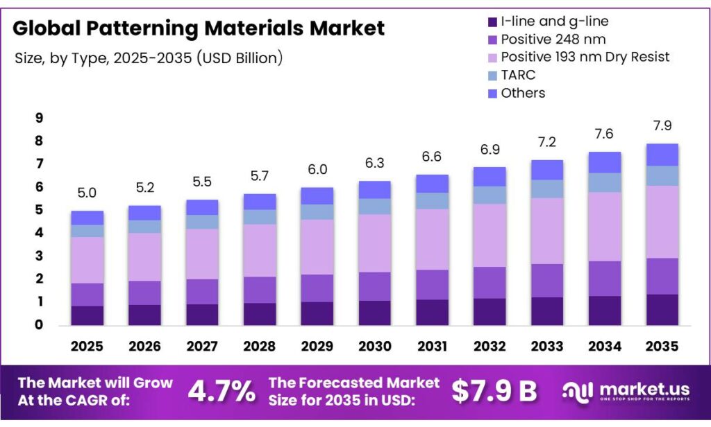
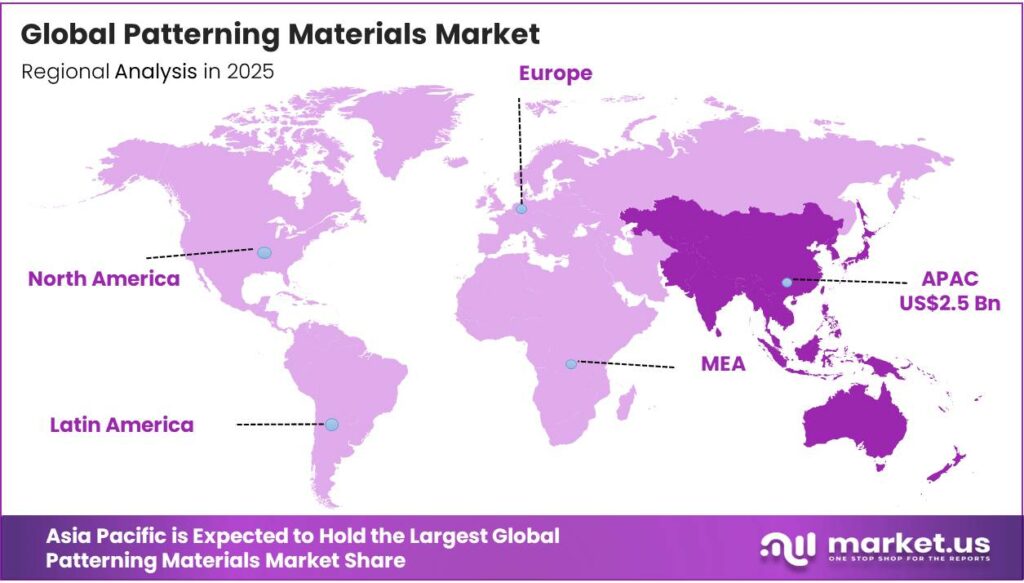
The Global Patterning Materials Market size is expected to be worth around USD 7.9 Billion by 2035, from USD 5.0 Billion in 2025, growing at a CAGR of 4.7% during the forecast period from 2026 to 2035. In 2025, Asia-Pacific held a dominant market position, capturing more than a 54.9% share, holding USD 4.5 Billion revenue.
The term patterning materials refers to substances used to create precise shapes, structures, or designs on a surface. As patterning is a core step in many industries, the specific materials used depend entirely on the field. The patterning materials market is fundamentally driven by semiconductor manufacturing intensity and lithographic complexity.
Core materials, such as photoresists, anti-reflective coatings, developers, and ancillary chemistries, are consumed across repeated lithography-etch cycles, often exceeding tens to over 100 patterned layers per device, linking demand directly to wafer throughput and device architecture. The transition to advanced nodes (sub-7 nm) and the growing adoption of EUV lithography are increasing material performance requirements, including higher sensitivity, lower line-edge roughness, and improved defect control.
However, cost and scalability constraints remain significant, as advanced lithography introduces higher process complexity and tighter integration tolerances. Concurrently, sustainability pressures, particularly around fluorinated chemistries and water-intensive processes, are driving innovation in greener formulations and recycling systems. Geopolitical factors, including export controls and supply-chain localization, are further reshaping sourcing and production strategies.
Regionally, Asia-Pacific dominates due to its concentration of fabrication capacity and materials supply. The market is characterized by high technical barriers, strong fab-supplier co-development, and continuous material innovation aligned with node scaling.
Key Takeaways
- The global patterning materials market was valued at US$5.0 billion in 2025.
- The global patterning materials market is projected to grow at a CAGR of 4.7% and is estimated to reach US$7.9 billion by 2035.
- Based on the types of patterning materials, positive 193 nm dry resist materials dominated the market, with a market share of around 39.8%.
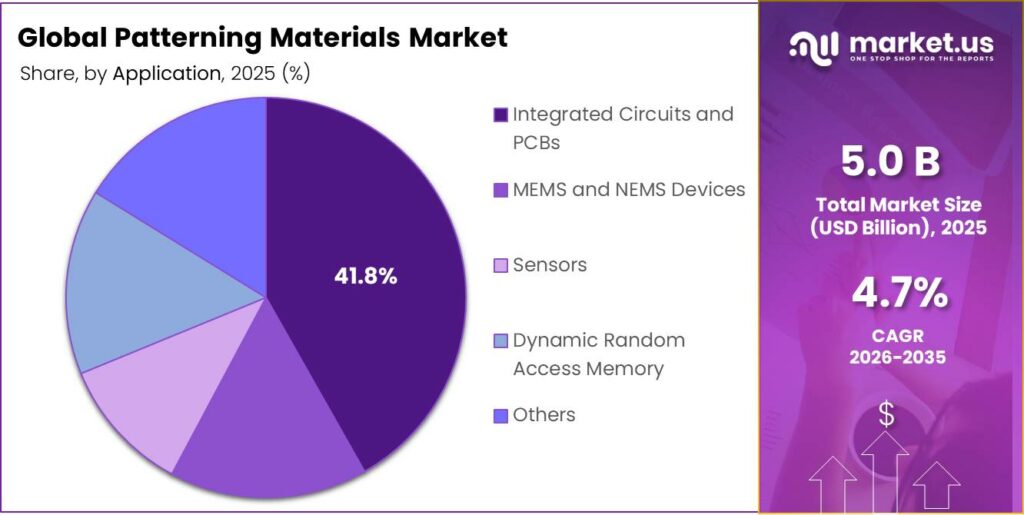
- Among the applications of patterning materials, integrated circuits and PCBs held a major share in the market, 41.8% of the market share.
- In 2025, the Asia Pacific was the most dominant region in the patterning materials market, accounting for around 51.2% of the total global consumption.
Type Analysis
Positive 193 nm Dry Resist Materials Held the Largest Share in the Patterning Materials Market.
The patterning materials market is segmented based on compound type into I-line and g-line, positive 248 nm, positive 193 nm dry resist, TARC, and others. The positive 193 nm dry resist materials dominated the market, comprising around 39.8% of the market share, as they provide an optimal balance of resolution, process maturity, and cost-effectiveness for high-volume semiconductor manufacturing. The shorter 193 nm wavelength (ArF lithography) enables significantly finer critical dimensions than i-line (365 nm), g-line (436 nm), or 248 nm (KrF) systems, making them suitable for sub-100 nm and even advanced multi-patterning applications.
Compared to immersion or EUV resists, 193 nm dry processes are simpler to integrate, avoiding added complexity such as fluid handling or stochastic defect challenges, while delivering high pattern fidelity. Positive-tone chemistry further supports better line-edge definition and process control in dense patterns. Additionally, the technology benefits from a well-established infrastructure, including exposure tools, track systems, and material supply chains, resulting in high throughput and yield stability.
Application Analysis
Patterning Materials Are Mostly Utilized for Integrated Circuits and PCBs.
Based on the applications of patterning materials, the market is divided into integrated circuits and PCBS, MEMS and NEMS devices, sensors, dynamic random access memory, and others. The integrated circuits and PCBS dominated the patterning materials market, with a market share of 41.8%, as these segments combine extreme volume, high layer counts, and standardized process flows, which drive repetitive and large-scale lithography usage. Advanced IC fabrication can involve tens to more than 100 patterned layers per wafer, each requiring photoresists, anti-reflective coatings, and developers, thereby multiplying material consumption per unit. PCB manufacturing, while less complex, is produced in very high panel volumes with multiple imaging and etching steps.
In contrast, MEMS/NEMS and sensors are typically fabricated in lower volumes with more heterogeneous designs and often use thicker resists or specialty processes, limiting throughput and standardization. Although DRAM is a major IC category, it represents a subset of the broader IC market, whereas logic and foundry applications span a wider range of devices and nodes. The scale, repetition, and process uniformity in ICs and PCBs structurally concentrate patterning material demand in these applications.
Key Market Segments
By Type
- I-line and g-line
- Positive 248 nm
- Positive 193 nm Dry Resist
- TARC
- Others
By Application
- Integrated Circuits and PCBs
- MEMS and NEMS Devices
- Sensors
- Dynamic Random Access Memory
- Others
Drivers
Expansion of the Semiconductor Industry Drives the Patterning Materials Market.
The expansion of the semiconductor industry and the continuous miniaturization of devices are primary catalysts for the patterning materials market. This relationship is governed by the technical requirements of advanced fabrication and the global scaling of production capacity. Device miniaturization, characterized by the progression of node sizes, necessitates more sophisticated patterning materials to maintain precision.
For instance, transistor counts have scaled from billions to over 15 billion in modern smartphones and hundreds of billions in AI data centers. Similarly, the industry has transitioned from 180 nm in 2000 to 7 nm in 2015, with 2 nm designs by 2025. According to the SEMI’s World Fab Forecast report, global fabrication capacity reached approximately 33.7 million wafers per month in 2025. Similarly, the Semiconductor Industry Association (SIA) announced global semiconductor sales hit US$791.7 billion in 2025, an increase of 25.6% compared to the 2024 total of US$630.5 billion.
Concurrently, miniaturization to sub-7 nm nodes requires higher-purity, chemically amplified resists and multi-patterning stacks. The EUV systems are indispensable for such nodes and enable significantly finer feature resolution. Technological progression to 3 nm nodes delivers performance gains over 5 nm, while next-generation High-NA EUV tools can shrink feature dimensions, increasing patterning complexity and material intensity per layer. The volumetric fab expansion and nanoscale pattern fidelity requirements act as primary, mutually reinforcing drivers of the patterning materials market.
Restraints
High Manufacturing Costs & Scaling Challenges Might Hamper the Demand for Patterning Materials.
High manufacturing costs and scaling complexities in advanced lithography constitute material constraints for the patterning materials market, particularly at leading-edge nodes. The cost of extreme ultraviolet (EUV) lithography systems, central to sub-7 nm patterning, is very high, reflecting extreme engineering complexity and capital intensity. Additionally, per-exposure costs for High-NA EUV are about 2.5 times higher than conventional EUV, increasing the cost per patterned layer.
Moreover, scaling further exacerbates process complexity. The advanced chips comprise about 100-150 patterned layers, many requiring multiple exposures or multi-patterning, which increases defect probability and material consumption per wafer. While High-NA EUV can reduce multi-patterning steps, it introduces new requirements such as redesigned photomasks and tighter process control, elevating integration costs.
Additionally, wafer fabrication costs escalate sharply with node scaling. For instance, leading-edge 3 nm wafers can exceed cost per wafer, compared to cost at 28 nm, indicating cost intensification tied to advanced patterning requirements. The high capital expenditure, rising per-layer processing costs, and integration challenges constrain scalable adoption of advanced patterning materials.
Opportunity
Shift Towards Sustainable Materials Creates Opportunities in the Patterning Materials Market.
The transition to sustainable patterning materials represents a strategic pivot for the semiconductor industry, primarily driven by intensifying global regulations on persistent chemicals and the sector’s decarbonization commitments. For instance, global regulatory bodies are moving to restrict Per- and Polyfluoroalkyl Substances (PFAS), which are historically foundational to photoresists, antireflective coatings, and rinses due to their specialized surface tension and thermal properties.
Similarly, a 2023 proposal by five European nations to the European Chemicals Agency (ECHA) seeks to restrict over 10,000 PFAS substances. While a 13.5-year derogation has been proposed for semiconductor manufacturing, the mandate necessitates a phased transition to PFAS-free alternatives. Similarly, under TSCA Section 8(a)(7), the EPA requires manufacturers to report PFAS usage dating back to 2011, with submission periods starting in April 2026.
Furthermore, the shift creates a market for green lithography chemistries that balance environmental compliance with the performance requirements of advanced nodes. Research institutes such as IMEC are actively developing PFAS-free chemically amplified resists (CARs) and metal-oxide resists (MOR) for EUV applications.
Transitioning from DUV to EUV lithography can reduce mask counts, which in some configurations led to a 21.9% decrease in PFAS-containing chemical consumption. Moreover, the industry targets a 43% reduction in greenhouse gas (GHG) emissions to meet 1.5°C climate goals. Sustainable materials, including those with lower global warming potential (GWP) and those enabling lower-energy processing, are critical to closing a projected 60 million metric ton CO₂e shortfall in the path to net-zero.
These dynamics are catalyzing R&D in greener photoresists, solvent systems, and pattern transfer techniques, positioning sustainability-driven material innovation as a key enabler of next-generation lithography ecosystems.
Trends
High Adoption of EUV Lithography.
The adoption of Extreme Ultraviolet (EUV) lithography has emerged as a definitive trend in semiconductor patterning, driven by the industry’s transition to sub-7nm process nodes. This shift creates a fundamental requirement for new classes of sensitive materials capable of resolving features at significantly smaller wavelengths. EUV technology utilizes a wavelength of 13.5 nm, a nearly 14-fold reduction compared to the 193 nm used in traditional Deep Ultraviolet (DUV) lithography.
Current EUV systems enable high-volume manufacturing for nodes at 14 nm and below. The industry is actively transitioning toward High Numerical Aperture (High-NA) EUV (0.55 NA), which is capable of resolving line-space patterns at an 8 nm half-pitch (HP). This progression necessitates the development of specialized Inorganic Metal Oxide Resists to manage stochastic effects and maintain etch resistance at extreme resolutions.
This transition intensifies requirements for advanced photoresists, pellicles, and defect-control materials due to higher photon energy, stochastic effects, and tighter line-edge roughness tolerances. Consequently, EUV adoption is directly reshaping material specifications and increasing technical sophistication across the patterning materials value chain.
Geopolitical Impact Analysis
Geopolitical Tensions Are Impacting the Patterning Materials Majorly Through Trade Restrictions.
The geopolitical tensions are materially reshaping the patterning materials market through trade restrictions, supply-chain fragmentation, and resource nationalism. Export controls introduced since 2022 restrict access to advanced semiconductor manufacturing equipment and related materials, particularly targeting China’s ability to produce sub-10 nm chips. These controls extend to lithography ecosystems, including photoresists and patterning chemistries linked to advanced nodes, constraining technology transfer and material standardization across regions.
Simultaneously, countermeasures on critical raw materials are intensifying supply risks. China accounted for about 99% of global gallium supply in 2024 and imposed export licensing controls, while prices for key inputs such as gallium increased in 2025 amid geopolitical disruptions. Such materials are integral to semiconductor fabrication and indirectly affect upstream patterning chemical supply chains.
Policy-driven localization further alters market structure. For instance, China’s requirement for up to 50% domestic equipment usage in new fabs is accelerating substitution of foreign inputs, while initiatives such as the European Chips Act aim to reduce external dependencies. Additionally, increasingly complex regulatory regimes are elevating qualification costs and extending material approval cycles. Collectively, these factors are fragmenting supply chains, increasing input volatility, and driving regionalization in the patterning materials ecosystem.
Regional Analysis
Asia Pacific Held the Largest Share of the Global Patterning Materials Market.
In 2025, the Asia Pacific dominated the global patterning materials market, holding about 51.2% of the total global consumption. The region constitutes the largest locus for patterning materials consumption due to its concentration of semiconductor fabrication capacity and advanced-node manufacturing. Taiwan, South Korea, China, and Japan collectively account for the majority of global wafer production. For instance, TSMC operates the world’s largest foundry network, producing over 12 million 12-inch-equivalent wafers annually, with EUV-based nodes concentrated in Taiwan. Similarly, Samsung Electronics maintains leading-edge fabrication lines in South Korea, integrating EUV lithography for sub-7 nm production.
China’s scale is expanding through state-backed capacity additions. Japan remains critical in upstream supply, as firms such as JSR Corporation and Tokyo Ohka Kogyo supply a substantial share of global photoresists and ancillary materials. Additionally, South Korea’s Ministry of Trade reports semiconductor exports exceeding 20% of national exports, reflecting sustained fabrication intensity. This geographic clustering of fabrication, materials production, and supply-chain integration structurally anchors Asia-Pacific as the dominant market for patterning materials.
Key Regions and Countries
- North America
- The US
- Canada
- Europe
- Germany
- France
- The UK
- Spain
- Italy
- Russia & CIS
- Rest of Europe
- APAC
- China
- Japan
- South Korea
- India
- ASEAN
- Rest of APAC
- Latin America
- Brazil
- Mexico
- Rest of Latin America
- Middle East & Africa
- GCC
- South Africa
- Rest of MEA
Key Players Analysis
Manufacturers of patterning materials focus on tightly coupled technology, supply-chain, and customer-integration strategies to sustain competitiveness. A primary priority is R&D intensity, particularly for EUV-compatible photoresists, low line-edge roughness formulations, and high-sensitivity chemistries that reduce stochastic defects. Additionally, firms pursue co-development with semiconductor fabs, embedding materials early into process integration flows to meet node-specific requirements and shorten qualification cycles.
Process-specific customization, including tailored resists, anti-reflective coatings, and developers for distinct lithography stacks, enhances switching costs and customer retention. Manufacturing localization near fabrication clusters improves supply assurance and compliance with regional regulations. Similarly, companies invest in high-purity production and contamination control systems, given sub-nanometer defect tolerances. Strategic activities further include intellectual property expansion, secure sourcing of specialty chemicals, and sustainability initiatives such as PFAS reduction and solvent recycling to align with tightening environmental standards.
The following are some of the major players in the industry
- Allresist GmbH
- Applied Materials, Inc.
- Brewer Science Inc.
- DONGJIN SEMICHEM CO., LTD
- DuPont
- Fujifilm Holdings Corporation
- Honeywell Electronic Materials, Inc.
- JSR Corporation
- MacDermid, Inc.
- Microchem Corporation
- Nissan Chemical Corporation
- Samsung SDI
- Shin-Etsu Chemical Co., Ltd.
- TOK TAIWAN CO., LTD.
- Tokyo Ohka Kogyo Co., Ltd.
- Other Key Players
Key Development
- In February 2024, Applied Materials, Inc. unveiled a portfolio of products and solutions aimed at meeting the advanced patterning demands of semiconductor manufacturing in the angstrom era.
- In July 2023, Brewer Science, Inc., a global leader in the development and manufacture of advanced materials for the microelectronics and optoelectronics industries, announced a significant advancement in high-temperature gap-filling materials. The company introduced OptiStack SOC450, a solution designed to support advanced process nodes by delivering exceptional performance under extreme temperature conditions.
Report Scope
| Report Features | Description |
|---|---|
| Market Value (2025) | US$5.0 Bn |
| Forecast Revenue (2035) | US$7.9 Bn |
| CAGR (2026-2035) | 4.7% |
| Base Year for Estimation | 2025 |
| Historic Period | 2020-2024 |
| Forecast Period | 2026-2035 |
| Report Coverage | Revenue Forecast, Market Dynamics, Competitive Landscape, Recent Developments |
| Segments Covered | By Type (I-line and g-line, Positive 248 nm, Positive 193 nm Dry Resist, TARC, and Others), By Application (Integrated Circuits and PCBs, MEMS and NEMS Devices, Sensors, Dynamic Random Access Memory, and Others) |
| Regional Analysis | North America – The US & Canada; Europe – Germany, France, The UK, Spain, Italy, Russia & CIS, Rest of Europe; APAC– China, Japan, South Korea, India, ASEAN & Rest of APAC; Latin America– Brazil, Mexico & Rest of Latin America; Middle East & Africa– GCC, South Africa, & Rest of MEA |
| Competitive Landscape | Allresist GmbH, Applied Materials, Inc., Brewer Science Inc., Dongjin Semichem Co., Ltd., DuPont, Fujifilm Holdings Corporation, Honeywell Electronic Materials, Inc., JSR Corporation, MacDermid, Inc., Microchem Corporation, Nissan Chemical Corporation, Samsung SDI, Shin-Etsu Chemical Co., Ltd., TOK Taiwan Co., Ltd., Tokyo Ohka Kogyo Co., Ltd., and Other Players. |
| Customization Scope | Customization for segments, region/country-level will be provided. Moreover, additional customization can be done based on the requirements. |
| Purchase Options | We have three licenses to opt for: Single User License, Multi-User License (Up to 5 Users), Corporate Use License (Unlimited Users and Printable PDF) |


