
Quick Navigation
Report Overview
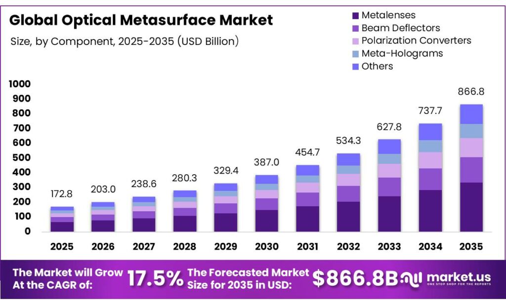
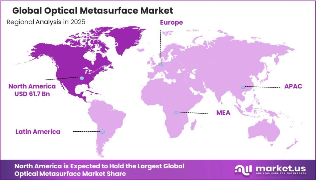
The Global Optical Metasurface Market size is expected to be worth around USD 866.8 Billion by 2035, from USD 172.8 Billion in 2025, growing at a CAGR of 17.5% during the forecast period from 2026 to 2035. In 2025, North America held a dominant market position, capturing more than a 43.7% share, holding USD 0.9 Billion revenue.
An optical metasurface is an ultra-thin, flat optical element composed of millions of tiny, sub-wavelength nanostructures called meta-atoms. Its market is characterized by the development and deployment of subwavelength, planar nanostructures that manipulate light in amplitude, phase, and polarization within ultrathin form factors. The technology is progressing from laboratory-scale demonstrations toward integration in commercial optical systems, particularly in applications requiring compact and multifunctional optics.
Demand is primarily driven by consumer electronics, especially AR/VR and imaging modules, where metasurfaces such as metalenses replace conventional multi-element lens assemblies. This enables reduced device thickness, simplified assembly, and enhanced optical functionality. Healthcare and biophotonics represent another growing application area, leveraging metasurfaces for high-sensitivity biosensing and miniaturized imaging systems.
However, the market faces constraints related to nanofabrication scalability, yield control, and material processing, as features often require sub-200 nm precision. Dielectric metasurfaces dominate due to their lower optical losses and compatibility with semiconductor manufacturing processes. Geopolitical factors, supply chain dependencies, and access to advanced lithography infrastructure further influence production and localization strategies. The market is transitioning from research-intensive development to application-driven commercialization.
Key Takeaways
- The global optical metasurface market was valued at US$172.8 billion in 2025.
- The global optical metasurface market is projected to grow at a CAGR of 17.5% and is estimated to reach US$866.8 billion by 2035.
- On the basis of components, metalenses dominated the market, constituting 38.6% of the total market share.
- Based on the materials of optical metasurfaces, dielectric metasurfaces dominated the market, with a substantial market share of around 47.8%.
- Based on the end-uses, the commercial sector led the optical metasurface market, comprising 57.9% of the total market.
- In 2025, North America was the most dominant region in the optical metasurface market, accounting for 35.7% of the total global consumption.
Component Analysis
Metalenses are a Prominent Segment in the Optical Metasurface Market.
The market is segmented based on components of the optical metasurfaces into metalenses, beam deflectors, polarization converters, meta-holograms, and others. The metalenses led the optical metasurface market, comprising 38.6% of the market share, as they directly substitute conventional refractive lens stacks in high-volume systems, especially imaging and sensing modules.
Unlike beam deflectors or polarization converters, which perform single optical functions, metalenses provide full wavefront control, enabling focusing, aberration correction, and compact imaging within a single planar element. This functional consolidation reduces component count, alignment steps, and form factor, which are critical constraints in consumer electronics and compact optical systems.
In contrast, components such as meta-holograms or polarization converters are often application-specific and lack comparable deployment breadth, limiting their integration into mass-produced optical architectures.
Material Analysis
Dielectric Metasurfaces Dominated the Optical Metasurface Market.
On the basis of the material, the optical metasurface market is segmented into dielectric metasurfaces, metallic metasurfaces, and hybrid metasurfaces. The dielectric metasurfaces dominated the optical metasurface market, comprising 47.8% of the market share, as they offer higher optical efficiency and lower losses than metallic (plasmonic) designs. Metals exhibit strong ohmic absorption at optical frequencies, which dissipates energy as heat and reduces transmission or reflection efficiency.
In contrast, high-index dielectric materials support Mie resonances with minimal absorption, enabling near-unity transmission efficiency and high phase coverage across visible and near-infrared wavelengths. Similarly, they are more compatible with semiconductor fabrication. Dielectric structures can be patterned using CMOS-aligned processes, supporting wafer-level manufacturing and integration with imaging sensors. Additionally, dielectric metasurfaces provide broadband operation and polarization control without requiring complex multilayer stacks.
Application Analysis
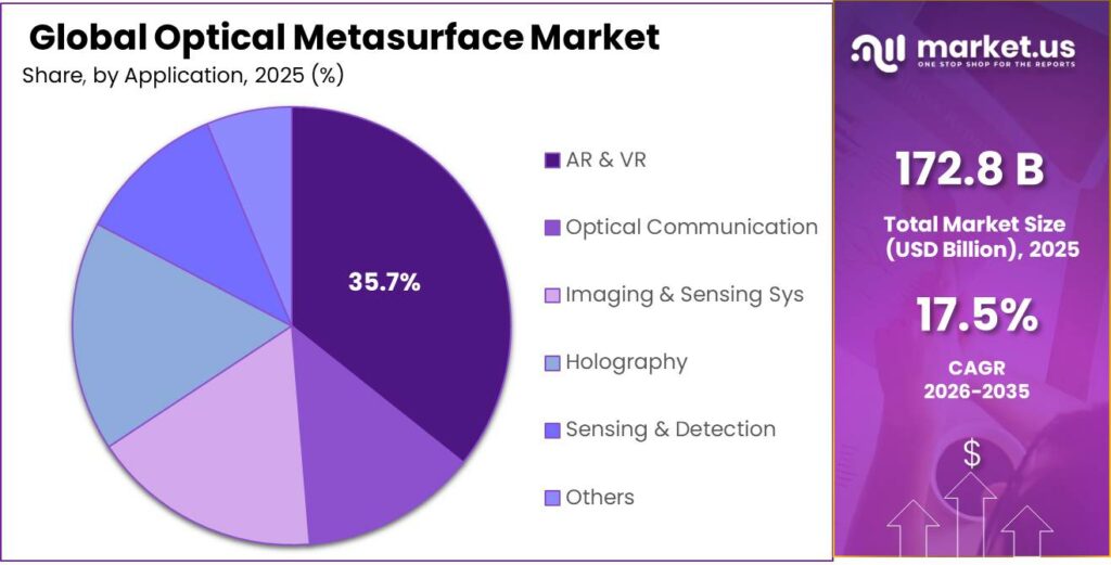
Optical Metasurface Products Are Mostly Utilized for AR & VR.
Based on the applications of the optical metasurface, the market is divided into AR & VR, optical communication, imaging & sensing sys, holography, sensing & detection, and others. AR & VR dominated the optical metasurface market, with a notable market share of 35.7%, as these systems impose strict constraints on size, weight, and optical form factor, where metasurfaces provide clear advantages by replacing bulky lens assemblies with ultrathin, planar components.
AR/VR headsets require compact optics to maintain ergonomics, and metasurfaces enable wavefront shaping, beam steering, and pupil expansion within millimeter-scale thicknesses. In addition, AR/VR applications typically operate in controlled illumination and display conditions, which align well with the narrowband or engineered spectral response of many metasurface designs. Integration with microdisplays and waveguides further benefits from flat optics that can be fabricated at the wafer scale. By contrast, optical communication systems often prioritize low loss over long distances, where metasurfaces face coupling and insertion loss challenges. Other applications, such as imaging or holography, require broader bandwidths, higher tolerance to fabrication variation, or larger apertures, which can be more demanding for metasurface implementation.
End-Use Analysis
The Commercial Sector Held a Major Share of the Optical Metasurface Market.
Among the end-uses, 57.9% of the total global consumption of optical metasurfaces is in the commercial sector, as they are designed to address integration, miniaturization, and form-factor constraints that are most critical in mass-produced products. Commercial applications, such as consumer electronics and compact sensing modules, benefit directly from metasurfaces’ ability to replace multi-element optical assemblies with a single planar device, simplifying assembly and reducing system complexity.
In contrast, industrial systems often prioritize robustness under harsh environments and long operational lifetimes, where metasurfaces still face challenges in durability and large-aperture scaling. Research and academia, while actively advancing the technology, typically focus on prototyping and experimental validation rather than deployment. Consequently, commercialization is driven by use cases where compactness, integration, and manufacturability provide immediate functional advantages.
Key Market Segments
By Component
- Metalenses
- Beam Deflectors
- Polarization Converters
- Meta-Holograms
- Others
By Material
- Dielectric Metasurfaces
- Metallic Metasurfaces
- Hybrid Metasurfaces
By Application
- AR & VR
- Optical Communication
- Imaging & Sensing Sys
- Holography
- Sensing & Detection
- Others
By End-Use
- Commercial
- Industrial
- Research & Academia
- Others
Drivers
Demand from Consumer Electronics Drives the Optical Metasurface Market.
The consumer electronics sector serves as a primary commercial driver for optical metasurfaces, shifting optics from traditional refractive elements to semiconductor-based planar components. This transition is characterized by the replacement of complex, multi-element lens stacks with single-layer meta-optics to achieve device miniaturization and enhanced sensing.
The primary market integration began in June 2022 with the release of the VL53L8 direct Time-of-Flight (dToF) sensor, developed through a partnership between STMicroelectronics and Metalenz. This marked the first commercial use of metasurfaces in consumer devices.
- By July 2025, STMicroelectronics reported shipping over 140 million metasurface optics and FlightSense modules.
Demand from consumer electronics is a primary driver of optical metasurface deployment, anchored in miniaturization and functional integration requirements. Metasurfaces reduce lens size to as little as 1/10,000th of traditional optics, combining the functionality of 3-4 complex lenses into a single flat layer. Similarly, the manufacturing has moved to 300mm semiconductor wafers, utilizing standard lithographic processes to align optics production with electronic chip fabrication.
In structured light systems, meta-optics project dot patterns with higher efficiency and wider fields of view compared to conventional diffractive optics. The convergence of semiconductor-compatible manufacturing and high-volume consumer electronics demand thus constitutes a demonstrable, non-speculative adoption pathway.
Restraints
Manufacturing and Scalability Issues Might Pose a Challenge to the Optical Metasurface Market.
The scalability of the optical metasurface market is fundamentally constrained by the technical requirements of high-aspect-ratio (HAR) nanopatterning and the throughput limitations of conventional lithography. Traditional methods such as electron beam lithography (EBL) and focused ion beam (FIB) milling offer sub-10 nm precision but are restricted by serial, point-by-point writing. Processing a single 12-inch wafer via EBL can take several days, rendering it unsuitable for industrial mass production.
Similarly, transitioning to nanoimprint lithography (NIL) increases throughput by more than 100 times compared to EBL at approximately 1/20th of the cost. However, resin-based NIL often suffers from low optical efficiency, under 10%, due to low refractive indices requiring additional complex processing to enhance performance. Wafer-level production demands consistent performance for every single device among the thousands produced on the same wafer, necessitating advanced metrology and tight process tolerances. Small deviations in nanostructure dimensions or etch profiles can significantly degrade optical efficiency, indicating high sensitivity to fabrication errors.
Material and process integration further complicates scaling. For instance, high-index materials such as TiO₂ require precise deposition and etching, with associated environmental and process challenges. Alternative methods improve throughput but face trade-offs between resolution, cost, and defect control. These constraints impede reliable, large-area, high-yield manufacturing.
Opportunities
Focus on the Active and Reconfigurable Metasurfaces to Create Opportunities in the Optical Metasurface
Active and reconfigurable metasurfaces represent a shift from static optical components to dynamic systems capable of real-time wavefront modulation. This functionality is achieved by integrating functional materials, such as phase-change materials (PCMs), liquid crystals, or elastomers, that respond to external electrical, thermal, or mechanical stimuli.
Research published by the U.S. Naval Research Laboratory (NRL) and DARPA-funded programs demonstrates that chalcogenide PCMs, such as GST, can switch refractive indices by over 2.0 upon heating. This allows a single metasurface to transition between a lens and a window in sub-microsecond timeframes. Active surfaces utilizing liquid crystal on silicon (LCoS) integration have achieved non-mechanical steering angles exceeding 60 degrees with diffraction efficiencies above 30%, addressing limitations in traditional LiDAR systems.
Similarly, electrically tunable metasurfaces developed in institutional collaborations have demonstrated focal length shifts of up to 20% by applying voltages under 10V, enabling ultra-compact autofocus without moving parts. Furthermore, the European Research Council (ERC) and National Science Foundation (NSF) have documented the transition toward CMOS-integrated active optics. By embedding electrodes directly into the metasurface backplane, developers can achieve pixel-level control of light, facilitating high-speed spatial light modulation for holographic displays and secure free-space optical communications.
Trends
Adoption of Optical Metasurface in Healthcare and Biophotonics.
The adoption of optical metasurfaces in healthcare is driven by the demand for miniaturized, high-resolution diagnostic tools and portable biophotonic sensors. By replacing bulky glass optics with planar meta-optics, medical devices achieve significant reductions in form factor while maintaining or enhancing optical performance.
Research institutions, including the National Institutes of Health (NIH) and Harvard SEAS, have demonstrated metalens-based endoscopes with diameters under 500 micrometers. These devices provide diffraction-limited imaging across the visible spectrum, overcoming the chromatic aberration typical of traditional refractive microlenses. Similarly, in Optical Coherence Tomography (OCT) applications, metasurfaces have achieved a depth of focus 10 times greater than conventional lenses, facilitating higher-resolution subsurface tissue mapping.
Furthermore, metasurface-based surface-enhanced Raman spectroscopy (SERS) substrates, as documented by the National Science Foundation (NSF), have shown limit-of-detection (LoD) improvements reaching attomolar levels for specific protein biomarkers. Using anisotropic nano-antennas, single-chip metasurfaces can simultaneously detect multiple pathogens by analyzing distinct polarization states, reducing sample volume requirements to microliter scales. IMEC has disclosed progress in integrating metasurfaces directly onto CMOS image sensors for lab-on-a-chip applications, enabling real-time, lens-free digital pathology in point-of-care settings.
Geopolitical Impact Analysis
Disrupted Semiconductor Industry is Affecting Optical Metasurface Market Amid Geopolitical Tensions.
The geopolitical tensions, particularly U.S.-China technology restrictions, are materially reshaping the optical metasurface ecosystem through supply-chain fragmentation, equipment constraints, and material dependencies.
The export controls on advanced semiconductors and fabrication tools directly affect metasurface manufacturing, which relies on semiconductor lithography infrastructure. The U.S. restrictions introduced in 2022-2025 limit China’s access to advanced chips and lithography systems, contributing to a 17% decline in Chinese semiconductor output in early 2023. Since metasurfaces are fabricated using similar sub-micron processes, such constraints propagate to meta-optics production capacity and cross-border technology transfer.
Additionally, supply-chain concentration creates material risks. China produces around one-third of global mature-node chips and dominates the processing of critical minerals such as gallium and germanium used in photonics. In 2025, China imposed licensing requirements on rare-earth exports for chips, extending controls to upstream inputs. These measures can disrupt optical material availability for metasurface fabrication.
Furthermore, geopolitical decoupling is altering innovation pathways. Export controls have incentivized domestic substitution, with China advancing to 7 nm chip production despite restrictions, while policy targets include 30% localization of 20-14 nm equipment by 2025. These dynamics introduce fragmentation in manufacturing ecosystems, constrain access to critical inputs, and reconfigure global collaboration networks underpinning optical metasurface development.
Regional Analysis
North America Held the Largest Share of the Global Optical Metasurface Market.
In 2025, North America dominated the global optical metasurface market, holding about 35.7% of the total global consumption, defined by a dense concentration of high-tier research institutions, substantial federal R&D investment, and a robust semiconductor manufacturing base. The region’s market activity is primarily anchored in the United States, where strategic government programs transition lab-scale breakthroughs into industrial-scale production.
For instance, the EXTREME (Extreme Optics and Imaging) program by DARPA has been instrumental in developing EnMats (engineered optical materials) to reduce the size and weight of optical systems to a sugar-cube scale. Similarly, in 2025, the NSF invested over US$163 million through its future manufacturing (FM) program, supporting projects across 136 institutions and companies to advance semiconductor and critical material production. Specific grants, such as a US$1.5 million award to Myrias Optics in October 2025, target the mass production of polarization-controlled metasurfaces.
At the device level, North America-based firms have disclosed commercialization of metasurface-enabled optical components in consumer and sensing applications, demonstrating translation from lab-scale to volume manufacturing. These factors, federal funding, fabrication infrastructure, and early commercialization, underpin North America’s leading role in optical metasurface development and deployment.
Key Regions and Countries
- North America
- The US
- Canada
- Europe
- Germany
- France
- The UK
- Spain
- Italy
- Russia & CIS
- Rest of Europe
- APAC
- China
- Japan
- South Korea
- India
- ASEAN
- Rest of APAC
- Latin America
- Brazil
- Mexico
- Rest of Latin America
- Middle East & Africa
- GCC
- South Africa
- Rest of MEA
Key Players Analysis
Manufacturers of optical metasurfaces focus on a set of technology-centric and supply-chain strategies to strengthen competitiveness. A primary priority is advancing semiconductor-compatible fabrication to achieve wafer-level scalability and high yield, enabling integration with CMOS processes. In addition, firms emphasize performance differentiation through multifunctional designs, combining focusing, beam shaping, and polarization control within a single layer, to reduce system complexity in end applications.
Moreover, intellectual property development is another key activity, with extensive patenting of nanostructure geometries, materials, and design algorithms. Strategic collaborations with foundries, research institutions, and system integrators support co-development and faster validation in applications such as 3D sensing and imaging.
Additionally, companies invest in active and tunable metasurfaces to enable reconfigurable optics, and in packaging/integration capabilities to ensure reliability under real-world operating conditions, including thermal and environmental stability.
The Major Players in The Industry
- Metalenz
- STMicroelectronics
- Moxtek
- MetaOptics Technologies
- NIL Technology (NILT)
- Lumotive
- 2Pi Optics
- Tunoptix
- Kymeta Corporation
- Viavi Solutions
- Other Key Players
Key Development
- In August 2025, Metalenz, a company specializing in the innovation and commercialization of metasurface technology, announced the expansion of its product and patent portfolio. The updated portfolio included metasurface technologies and system-level applications designed for secure biometric solutions.
- In July 2025, Metalenz and STMicroelectronics (STM) entered into an expanded licensing agreement that permits STM to continue producing metasurface optics utilizing Metalenz’s intellectual property within its 300 mm semiconductor fabrication facilities.
Report Scope
| Report Features | Description |
|---|---|
| Market Value (2025) | US$172.8 Bn |
| Forecast Revenue (2035) | US$866.8 Bn |
| CAGR (2026-2035) | 17.5% |
| Base Year for Estimation | 2025 |
| Historic Period | 2020-2024 |
| Forecast Period | 2026-2035 |
| Report Coverage | Revenue Forecast, Market Dynamics, Competitive Landscape, Recent Developments |
| Segments Covered | By Component (Metalenses, Beam Deflectors, Polarization Converters, Meta-Holograms, and Others), By Material (Dielectric Metasurfaces, Metallic Metasurfaces, and Hybrid Metasurfaces), By Application (AR & VR, Optical Communication, Imaging & Sensing Sys, Holography, Sensing & Detection, and Others), By End-use (Commercial, Industrial, Research & Academia, and Others) |
| Regional Analysis | North America – The US & Canada; Europe – Germany, France, The UK, Spain, Italy, Russia & CIS, Rest of Europe; APAC– China, Japan, South Korea, India, ASEAN & Rest of APAC; Latin America– Brazil, Mexico & Rest of Latin America; Middle East & Africa– GCC, South Africa, & Rest of MEA |
| Competitive Landscape | Metalenz, STMicroelectronics, Moxtek, MetaOptics Technologies, NIL Technology (NILT), Lumotive, 2Pi Optics, Tunoptix, Kymeta Corporation, Viavi Solutions, and Other Players. |
| Customization Scope | Customization for segments, region/country-level will be provided. Moreover, additional customization can be done based on the requirements. |
| Purchase Options | We have three licenses to opt for: Single User License, Multi-User License (Up to 5 Users), Corporate Use License (Unlimited Users and Printable PDF) |


