
Quick Navigation
- Report Overview
- Semiconductor Prime Wafer Statistics
- Key Takeaways
- Regional Analysis
- By Wafer Size
- By Application
- By End User
- Key Market Segments
- Driving Factors
- Restraining Factors
- Growth Opportunities
- Challenging Factors
- Growth Factors
- Emerging Trends
- Business Benefits
- Key Players Analysis
- Recent Developments
- Report Scope
Report Overview
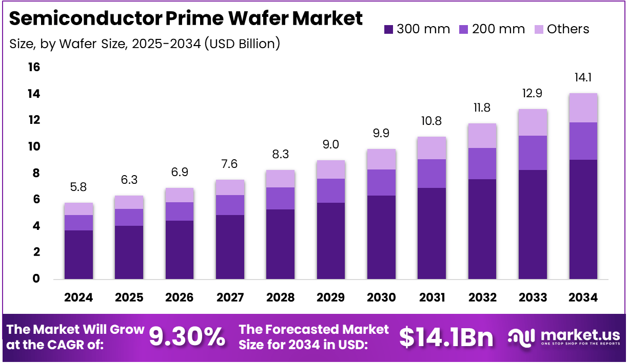
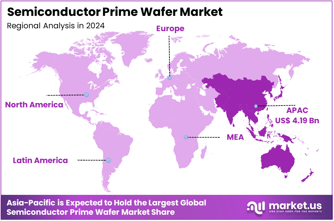
The Global Semiconductor Prime Wafer Market size is expected to be worth around USD 14.1 Billion By 2034, from USD 5.8 Billion in 2024, growing at a CAGR of 9.30% during the forecast period from 2025 to 2034. In 2024, Asia-Pacific held a dominant market position, capturing more than a 72.4% share, holding USD 4.19 Billion in revenue.
A semiconductor prime wafer is a high-quality silicon wafer used as the base for manufacturing integrated circuits (ICs). These wafers undergo rigorous processing to achieve exceptional flatness, cleanliness, and surface quality, which are crucial for photolithography and other vital semiconductor fabrication processes.
They are essential for creating advanced electronic devices, such as smartphones, computers, and automotive systems. In the global market, the semiconductor prime wafer market is an integral part of the semiconductor industry, focusing on the production and supply of these premium wafers.
The market’s growth is fueled by several factors, including technological advancements that have led to smaller and more efficient node technologies in semiconductor production. The rise in demand for consumer electronics, automotive electronics, and industrial systems that rely on sophisticated semiconductors is another major driving factor.
Semiconductor Prime Wafer Statistics
Global Shipment Data
- Total Shipments (Q3 2024): 3,214 million square inches (MSI), a 5.9% increase from the previous quarter and a 6.8% increase year-over-year.
- Projected Shipments (2024): Expected to decline by 2% to 12,174 MSI, with a rebound of 10% anticipated in 2025, reaching approximately 13,328 MSI.
Import and Export Data
- Total Import/Export Shipments (India): Total of 14,010 shipments from March 2023 to February 2024, reflecting a growth rate of 100%.
- Key Import Figures: Significant imports include various types of silicon wafers from China, such as undiffused monocrystalline and multicrystalline wafers.
Lifecycle and Production
- Wafer Sizes: Common sizes include 6-inch, 8-inch, and up to 12-inch wafers. The transition to larger wafer sizes is ongoing, with significant investments in production facilities for larger diameters.
Usage and Applications
- Primary Applications: Integrated Circuits, Solar Cells, Photoelectric Cells/
- Wafers Types: Polished Wafers are used in DRAM, LCD drivers, and flash memory, Epitaxial Wafers are used in image sensors and microprocessors.
As industries continue to innovate, particularly with the shift toward electric vehicles and smart manufacturing, the demand for semiconductor prime wafers is set to rise. Moreover, the expansion of renewable energy sources, such as solar and wind power, is increasing the need for semiconductors for efficient power conversion systems, further driving market growth.
There are numerous opportunities in the semiconductor prime wafer market, particularly in emerging markets like China and India, where rapid industrialization is spurring demand for high-quality semiconductors.
Additionally, the development of advanced packaging technologies and the deployment of 5G networks are creating new avenues for wafer manufacturers. As semiconductor technology continues to advance, including innovations like EUV lithography and the shift to larger wafer sizes, there are significant opportunities for growth.
Furthermore, new materials such as gallium nitride (GaN) and silicon carbide (SiC) are expanding the applications for prime wafers, particularly in power electronics and high-efficiency devices. Technological advancements in the semiconductor industry are playing a pivotal role in shaping the prime wafer market.
The industry is seeing a push towards smaller node technologies, with 5nm and 3nm chips requiring ultra-high-quality wafers to meet performance demands. The adoption of extreme ultraviolet (EUV) lithography is enabling the creation of smaller, more complex ICs, further driving the need for high-quality prime wafers.
Additionally, the movement towards larger wafer sizes, such as 450mm wafers, is aimed at increasing manufacturing efficiency, although it presents challenges in terms of wafer quality and handling. Innovations in automation and artificial intelligence in wafer production are also enhancing manufacturing efficiency, reducing defects, and improving overall yield, making the semiconductor prime wafer market even more dynamic.
Key Takeaways
- Market Growth: The Semiconductor Prime Wafer Market is expected to grow from USD 5.8 billion in 2024 to USD 14.1 billion by 2034, at a CAGR of 9.30%.
- By Wafer Size: The 300 mm wafer segment dominates, accounting for 64.3% of the market share, reflecting its widespread adoption in high-volume semiconductor production.
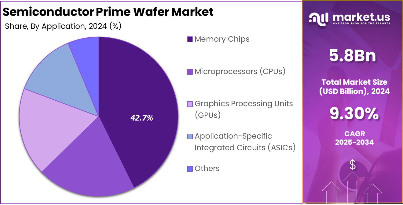
- By Application: Memory Chips lead the market with a 42.7% share, driven by their essential role in various electronic devices, from consumer electronics to industrial systems.
- By End User: Semiconductor Foundries represent the largest end-user segment, holding 78.4% of the market share, reflecting their key role in wafer production and semiconductor fabrication.
- Regional Insights: Asia Pacific dominates the market, capturing 72.4% of the market share, driven by significant semiconductor manufacturing activity in countries like China, South Korea, and Taiwan.
Regional Analysis
In 2024, Asia-Pacific held a dominant market position in the Semiconductor Prime Wafer Market, capturing more than 72.4% of the total market share, generating USD 4.19 billion in revenue. This region’s dominance can be attributed to its robust semiconductor manufacturing ecosystem, with key players like Taiwan, South Korea, China, and Japan driving significant production and demand for semiconductor wafers.
The region houses the world’s leading semiconductor foundries, including TSMC, Samsung Electronics, and SMIC, which significantly contribute to the high demand for prime wafers, particularly for memory chips and advanced ICs used in consumer electronics, automotive, and industrial applications. Asia-Pacific’s substantial market share is further supported by the rapid growth of the semiconductor industry in China, which is the largest consumer of semiconductor wafers.
China, in particular, has made substantial investments in expanding its semiconductor fabrication capacity, aligning with the country’s national ambitions to strengthen its self-sufficiency in advanced semiconductor manufacturing. Additionally, the increasing adoption of next-generation technologies such as 5G, IoT, and electric vehicles in the region is driving a surge in demand for high-quality wafers, boosting the market further.
By Wafer Size
In 2024, the 300 mm segment held a dominant market position in the Semiconductor Prime Wafer Market, capturing more than 64.3% of the total market share. The primary reason for the 300 mm wafer’s leadership is its widespread adoption in high-volume semiconductor manufacturing, particularly in the production of memory chips and integrated circuits (ICs) used in consumer electronics, automotive, and industrial applications.
The 300 mm wafer size allows for higher production efficiency and lower per-wafer costs, making it the preferred choice for semiconductor foundries. As the demand for smaller, more powerful electronic devices increases, the ability to produce more chips per wafer—combined with enhanced yield rates—has made 300 mm wafers the industry standard.
Additionally, advancements in photolithography and wafer processing technologies have further supported the transition to 300 mm wafers, which offer superior scalability for emerging technologies such as 5G, IoT, and AI applications. Consequently, the 300 mm segment continues to dominate due to its cost-effectiveness and efficiency in producing high-performance semiconductors at scale.
By Application
In 2024, the Memory Chips segment held a dominant market position in the Semiconductor Prime Wafer Market, capturing more than 42.7% of the total market share. The reason for the Memory Chips segment’s leadership is the critical role memory chips play in virtually every modern electronic device, from smartphones and computers to automotive systems and IoT devices.
As the demand for higher storage capacities and faster processing speeds continues to grow, particularly with the proliferation of data-intensive applications such as cloud computing, artificial intelligence (AI), and 5G, memory chips have become indispensable. These chips require high-quality semiconductor wafers for their production, driving substantial demand for semiconductor prime wafers.
Additionally, the continuous evolution of technologies like DRAM, NAND flash, and emerging memory types like 3D NAND has spurred growth in this segment. As a result, the memory chips segment remains the largest consumer of semiconductor prime wafers, with ongoing innovations aimed at improving performance and storage density further solidifying its market dominance.
By End User
In 2024, the Semiconductor Foundries segment held a dominant market position in the Semiconductor Prime Wafer Market, capturing more than 78.4% of the total market share. Semiconductor foundries are the backbone of global wafer production, and their dominance is primarily driven by their pivotal role in wafer fabrication and semiconductor manufacturing.
These foundries, such as TSMC, Samsung Electronics, and GlobalFoundries, are responsible for producing a large volume of semiconductor chips for a wide range of applications, including consumer electronics, automotive, and industrial sectors. Foundries are highly dependent on high-quality semiconductor prime wafers for producing advanced integrated circuits (ICs) and memory chips, which are critical components in modern electronic devices.
The increasing demand for cutting-edge technologies, such as 5G, AI, and IoT, has further boosted the reliance on semiconductor foundries. Additionally, the trend toward more sophisticated, smaller node processes and the growing need for mass production of semiconductors for various industries have solidified the semiconductor foundries segment as the leader in the market.
Key Market Segments
By Wafer Size
- 200 mm
- 300 mm
- Others
By Application
- Memory Chips
- Microprocessors (CPUs)
- Graphics Processing Units (GPUs)
- Application-Specific Integrated Circuits (ASICs)
- Others
By End User
- Semiconductor Foundries
- Integrated Device Manufacturers (IDMs)
- Others
Driving Factors
Surge in Demand for Advanced Consumer Electronics
The escalating demand for advanced consumer electronics is a significant driving force behind the growth of the semiconductor prime wafer market. Devices such as smartphones, tablets, wearables, and smart home appliances require sophisticated semiconductor components, which in turn depend on high-quality prime wafers for their production.
As consumers increasingly seek devices with enhanced performance, greater storage capacities, and improved functionalities, the need for advanced memory chips and microprocessors has surged. This trend has led to a substantial increase in the production of semiconductor wafers, as manufacturers strive to meet the evolving requirements of the consumer electronics sector.
Restraining Factors
Supply Chain Disruptions
Supply chain disruptions pose a significant challenge to the semiconductor prime wafer market. Events such as the COVID-19 pandemic have led to shortages of raw materials and delays in transportation, resulting in increased costs and reduced availability of silicon wafers.
These disruptions have affected manufacturers’ ability to maintain consistent production schedules, leading to potential delays in the delivery of semiconductor components to end-users. Additionally, geopolitical tensions and natural disasters can further exacerbate supply chain vulnerabilities, making it challenging for manufacturers to secure the necessary materials and components for wafer production.
The semiconductor industry is highly sensitive to such disruptions, as even minor delays can have cascading effects on the entire supply chain, impacting the timely availability of electronic devices in the market.
Growth Opportunities
Expansion in Automotive Electronics
The rapid advancement of automotive electronics presents a significant growth opportunity for the semiconductor prime wafer market. The automotive industry’s shift towards electric vehicles (EVs) and the integration of advanced driver-assistance systems (ADAS) have increased the demand for sophisticated semiconductor components.
These components, including power management ICs, sensors, and microcontrollers, are essential for the efficient operation of modern vehicles. As the automotive sector continues to embrace electrification and automation, the need for high-quality semiconductor wafers is expected to rise.
This trend offers manufacturers the opportunity to diversify their product offerings and tap into the growing automotive electronics market, which is projected to experience substantial growth in the coming years.
Challenging Factors
High Manufacturing Costs
High manufacturing costs present a significant challenge to the semiconductor prime wafer market. The production of high-quality wafers requires advanced technology and precision, leading to substantial capital investment. Smaller manufacturers may find it particularly challenging to invest in the necessary equipment and facilities, potentially limiting their ability to compete effectively in the market.
Additionally, fluctuations in raw material prices and energy costs can further increase production expenses, impacting profit margins. To remain competitive, manufacturers must continually invest in research and development to improve production efficiency and reduce costs.
However, such investments require significant financial resources, which may not be readily available to all companies, especially those operating on a smaller scale. This financial barrier can hinder market entry and expansion, limiting the overall growth potential of the industry.
Growth Factors
The increasing demand for consumer electronics is one of the primary growth drivers for the semiconductor prime wafer market. With global smartphone shipments surpassing 1.2 billion units in 2023, the need for high-performance semiconductor components has surged.
These devices, from smartphones to wearables, require advanced memory chips and microprocessors, which in turn depend on high-quality semiconductor wafers. As consumer electronics continue to evolve and demand more advanced features, manufacturers will need a consistent supply of prime wafers to meet the growing production requirements.
Another critical growth factor is the automotive industry’s shift toward electric vehicles (EVs) and the rising integration of advanced driver-assistance systems (ADAS). The automotive sector accounted for nearly 20% of the semiconductor wafer market share in 2023, and this figure is expected to rise as governments worldwide promote EV adoption.
The demand for power management ICs, sensors, and microcontrollers used in EVs and autonomous vehicles is driving the need for high-quality semiconductor wafers. This shift represents a significant growth opportunity for wafer manufacturers, as the automotive industry seeks to meet its evolving semiconductor needs.
Emerging Trends
One of the most notable trends in the semiconductor wafer market is the increasing adoption of 300mm wafers. In 2023, 300mm wafers accounted for 65% of total wafer production. These wafers are preferred for their ability to deliver higher yields and lower per-wafer costs compared to smaller wafer sizes, making them the standard in large-scale semiconductor production.
As demand for miniaturized and more powerful semiconductor devices grows, the shift toward 300mm wafers is expected to continue, driving further efficiency in wafer production. Another emerging trend is the integration of artificial intelligence (AI) and the Internet of Things (IoT) into semiconductor designs. AI and IoT technologies are creating the need for more advanced semiconductor components capable of supporting complex computations and real-time connectivity.
This shift is pushing wafer manufacturers to innovate and develop specialized wafers that can meet the unique demands of AI and IoT applications. As these technologies become more embedded in industries such as healthcare, automotive, and manufacturing, the demand for wafers tailored for AI and IoT is likely to grow rapidly.
Business Benefits
This growth is driven by increasing demand from industries such as consumer electronics, automotive, and industrial applications, where semiconductor components are integral to functionality. For wafer manufacturers, this expanding market provides substantial revenue potential, particularly as technological innovations and emerging sectors continue to drive the demand for advanced semiconductor devices.
Strategic partnerships also offer considerable business benefits in the semiconductor prime wafer market. Collaborations between semiconductor manufacturers and technology companies have become key drivers of innovation and market expansion.
For example, TSMC’s partnerships with leading tech firms have strengthened its market position and fueled its growth in advanced semiconductor manufacturing. These partnerships help companies stay competitive by enabling them to access cutting-edge technology, expand their market reach, and optimize their production capabilities, ultimately boosting profitability.
Key Regions and Countries
- North America
- US
- Canada
- Europe
- Germany
- France
- The UK
- Spain
- Italy
- Russia
- Netherlands
- Rest of Europe
- Asia Pacific
- China
- Japan
- South Korea
- India
- Australia
- Singapore
- Thailand
- Vietnam
- Rest of APAC
- Latin America
- Brazil
- Mexico
- Rest of Latin America
- Middle East & Africa
- South Africa
- Saudi Arabia
- UAE
- Rest of MEA
Key Players Analysis
Pure Wafer, a leading supplier of silicon wafer solutions in the United States, was acquired by ZMC, a New York-based private equity firm. This acquisition aims to drive a new growth phase for Pure Wafer, focusing on substantial investments in advanced technology and the expansion of fabrication capacity across its U.S. wafer operations. The goal is to meet the increasing demand from top semiconductor original equipment manufacturers (OEMs) and integrated device manufacturers (IDMs).
In June 2024, Shin-Etsu Chemical, a prominent Japanese chemical company, acquired all shares of Mimasu Semiconductor Industry for approximately $430.9 million, increasing its stake from 43.87% to 100%. This acquisition was aimed at enhancing Shin-Etsu Chemical’s electronic materials business by integrating MIMASU’s semiconductor-related services, including silicon wafer processing, industrial sales, and engineering.
As of the latest available information, there are no publicly disclosed details regarding recent acquisitions, new product launches, or mergers involving Wafer World Inc. The company continues to operate within the semiconductor wafer industry, providing a range of products and services to meet the needs of semiconductor manufacturers.
Top Key Players in the Market
- Pure Wafer
- Mimasu Semiconductor Industry
- Wafer World Inc.
- GlobalWafers
- RS Technologies
- Shin-Etsu Chemical
- Ecolab
- SK Siltron
- Wafer Works Corporation
- Other Major Players
Recent Developments
- In 2024, Pure Wafer, a leading player in the semiconductor prime wafer market, significantly expanded its operations in the United States following its acquisition by ZMC, a private equity firm.
- In 2024, Shin-Etsu Chemical, a leading global chemical company, completed the acquisition of Mimasu Semiconductor Industry, increasing its stake to 100%.
Report Scope
| Report Features | Description |
|---|---|
| Market Value (2024) | USD 5.8 Bn |
| Forecast Revenue (2034) | USD 14.1 Bn |
| CAGR (2025-2034) | 9.30% |
| Largest Market | North America |
| Base Year for Estimation | 2024 |
| Historic Period | 2020-2023 |
| Forecast Period | 2025-2034 |
| Report Coverage | Revenue Forecast, Market Dynamics, Competitive Landscape, Recent Developments |
| Segments Covered | By Wafer Size (200 mm, 300 mm, Others), By Application (Memory Chips, Microprocessors (CPUs), Graphics Processing Units (GPUs), Application-Specific Integrated Circuits (ASICs), Others), By End User (Semiconductor Foundries, Integrated Device Manufacturers (IDMs), Others) |
| Regional Analysis | North America (US, Canada), Europe (Germany, UK, Spain, Austria, Rest of Europe), Asia-Pacific (China, Japan, South Korea, India, Australia, Thailand, Rest of Asia-Pacific), Latin America (Brazil), Middle East & Africa(South Africa, Saudi Arabia, United Arab Emirates) |
| Competitive Landscape | Pure Wafer, Mimasu Semiconductor Industry, Wafer World Inc., GlobalWafers, RS Technologies, Shin-Etsu Chemical, Ecolab, SK Siltron, Wafer Works Corporation, Other Major Players |
| Customization Scope | We will provide customization for segments and at the region/country level. Moreover, additional customization can be done based on the requirements. |
| Purchase Options | We have three licenses to opt for Single User License, Multi-User License (Up to 5 Users), Corporate Use License (Unlimited User and Printable PDF) |


