Report Overview
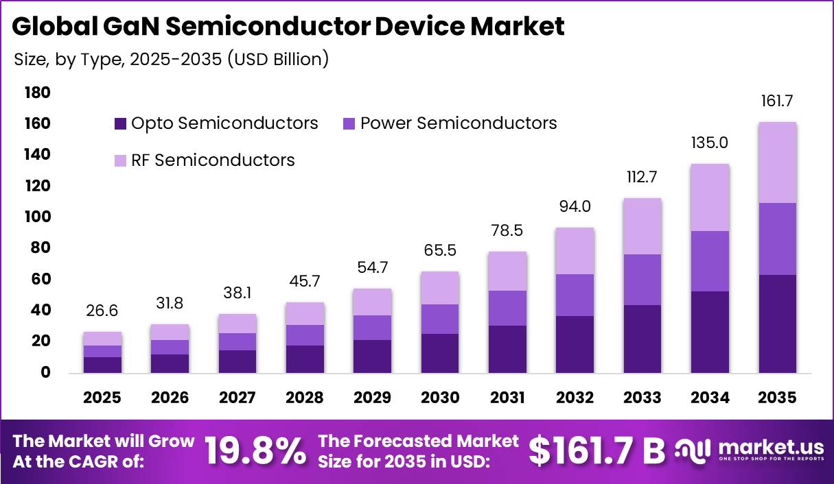
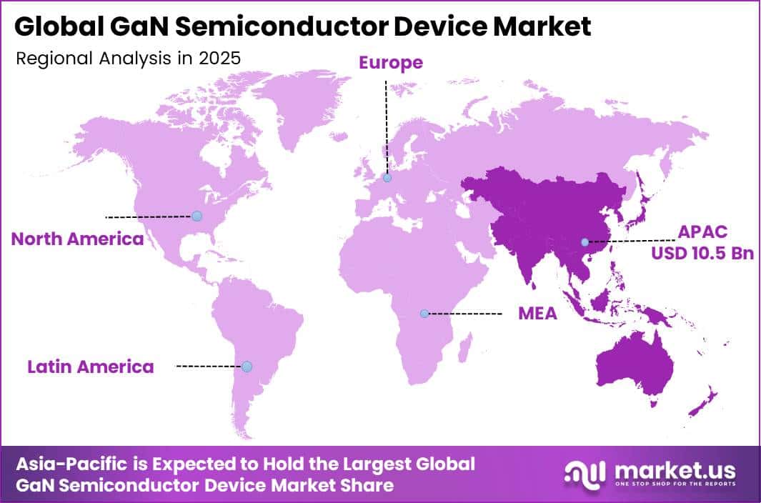
In 2025, the Global GaN Semiconductor Device Market was valued at USD 26.6 billion. The market is projected to grow at a CAGR of 19.8% during 2026–2035, reaching approximately USD 161.7 billion by 2035. Asia-Pacific dominated the global market in 2025, accounting for more than 39.4% of the total market share and generating approximately USD 10.5 billion in revenue.
Market growth is supported by increasing use of GaN devices in 5G infrastructure, electric vehicles, fast chargers, data centres, and renewable-energy systems. GaN devices offer faster switching and lower power losses compared with many conventional silicon devices, helping manufacturers build smaller and more energy-efficient chargers, power supplies, inverters, and radio-frequency systems.
In 2025, 5G networks covered about 55% of the global population and accounted for nearly 3 billion mobile-broadband subscriptions, creating strong demand for high-frequency GaN components in telecom equipment. 5G coverage reached about 70% of the Asia-Pacific population in 2025, compared with the global level of 55%.
Global electric-car sales also exceeded 20 million units in 2025, representing one in four new cars sold. Rising EV production supports demand for GaN-based onboard chargers and charging systems. In addition, around 4,600 GW of renewable capacity is expected to be added during 2025–2030, strengthening demand for efficient GaN power devices used in solar, wind, inverter, and grid applications.
Key Takeaway
- The GaN Semiconductor Device Market was valued at USD 26.6 billion in 2025 and is projected to reach USD 161.7 billion by 2035 at a CAGR of 19.8%.
- Opto semiconductors dominate the GaN semiconductor device market with a 39.1% share, supported by strong demand across LEDs, lasers, displays, and photodetectors.
- Transistors hold a leading 38.2% share, driven by their growing use in power conversion, RF systems, and high-efficiency electronics.
- The 4-inch wafer segment leads with a 35.5% share, supported by established production processes, stable yields, and controlled manufacturing costs.
- Consumer electronics accounts for a leading 28.6% share, fueled by high-volume demand for smartphones, laptops, displays, chargers, and power adapters.
- Asia-Pacific led the market in 2025 with a 39.4% share and about USD 10.5 billion in revenue.
By Type
Opto semiconductors held a dominant position in the GaN semiconductor device market, accounting for 39.1% of the market. This leadership is mainly supported by the wide use of GaN in light-emitting diodes, laser diodes, photodetectors, displays, automotive lighting, and ultraviolet lighting systems. GaN has a direct bandgap that allows efficient production of blue, green, and ultraviolet light.
NIST identifies GaN-based semiconductor technology as an important material for blue-green and UV lasers, LEDs, and photodetectors. Demand is also supported by the steady transition toward energy-efficient lighting systems. According to the U.S. Department of Energy, LED products represented more than 50% of the global lighting market in 2020 and 2021.
Their growing use across homes, commercial buildings, streetlights, vehicles, displays, and industrial facilities continues to create demand for GaN optoelectronic components. The U.S. Department of Energy further projects that LED lighting could represent around 84% of lighting installations by 2035, providing a strong long-term demand base for GaN optoelectronic semiconductor devices.
By Component
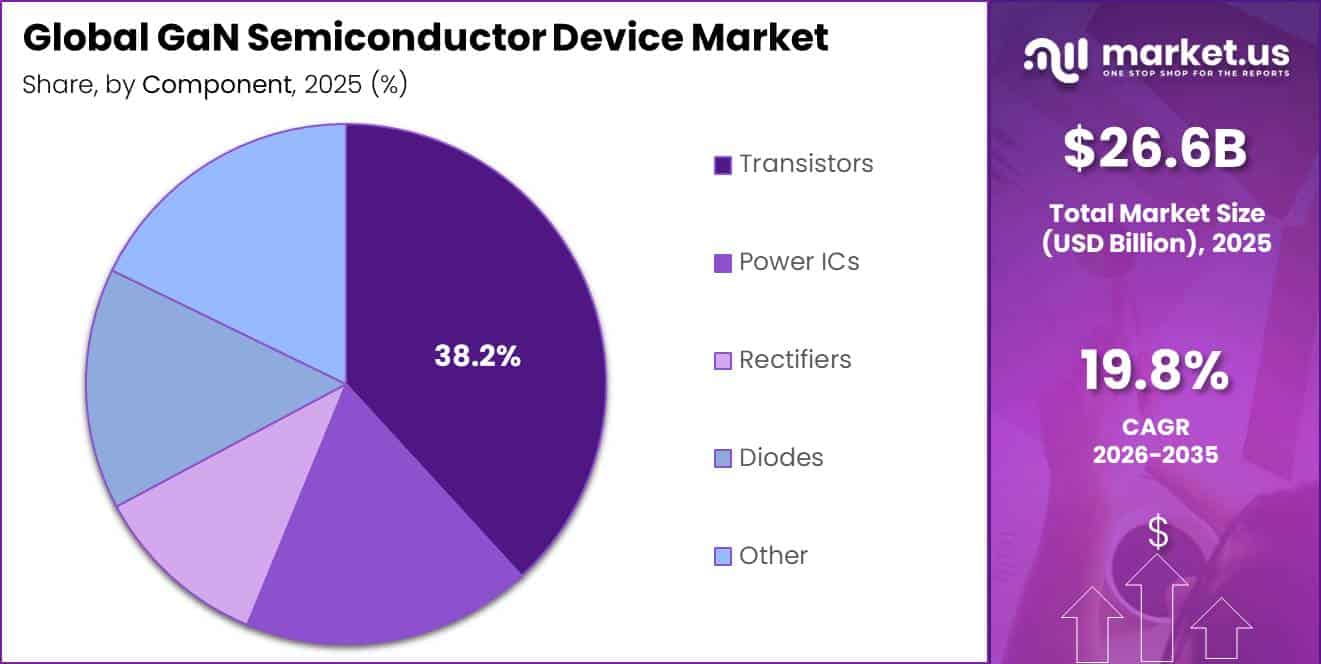
Transistors hold the leading position in the GaN semiconductor device market, accounting for a 38.2% share. Their strong market position comes from their important role as switching and control components in power converters, radio-frequency amplifiers, data-centre equipment, and high-density computing power supplies. Growing electricity use in data centres is creating a greater need for efficient power conversion technologies.
According to the International Energy Agency, data centres consumed around 415 TWh of electricity in 2024, while their electricity demand is expected to reach approximately 945 TWh by 2030. This sharp increase makes power efficiency increasingly important for controlling operating costs and reducing energy losses. GaN transistors can operate at much higher switching frequencies while generating lower losses than conventional silicon devices.
This allows manufacturers to design smaller power systems with reduced cooling and magnetic component requirements. The U.S. Department of Energy has also demonstrated GaN-based converters for data-centre applications targeting efficiency levels of more than 97%, highlighting the technology’s potential in advanced power infrastructure.
By Wafer Size
The 4-inch wafer segment holds a leading position in the GaN semiconductor device market, accounting for a 35.5% share. Its dominance is supported by its established use in GaN manufacturing, where producers can balance wafer quality, usable die output, process stability, and production risk.
This format remains particularly important for high-frequency and power devices, as lower defect levels can improve device yield and long-term reliability. According to modelling by the Japan Science and Technology Agency, the cost of a 4-inch GaN substrate is around JPY 400,000 per wafer. The substrate can also represent nearly 60% of the total manufacturing cost of a GaN MOSFET.
Due to this high cost contribution, manufacturers often continue using qualified 4-inch production lines rather than making expensive changes to larger wafer formats. Although larger wafers can reduce cost per device through higher production volume, challenges in GaN crystal growth, defect control, and manufacturing consistency continue to support demand for 4-inch wafers across commercial GaN device production.
By End-Use Industry
Consumer Electronics accounts for a leading 28.6% share of GaN semiconductor device demand, supported by the high production and replacement volumes of smartphones, laptops, tablets, displays, and charging devices. These products require compact, efficient, and lightweight power components, making GaN technology well suited for modern consumer applications.
According to ITU and UNITAR, small IT and telecommunications equipment, including mobile phones, laptops, and routers, generated around 4.6 million tonnes of electronic waste in 2022. This large replacement cycle creates recurring demand for new chargers, adapters, displays, and related semiconductor components.
GaN devices offer lower switching losses and can operate at higher frequencies than traditional silicon devices, allowing manufacturers to design smaller and cooler power adapters with improved energy efficiency. A NIST Manufacturing USA report also highlights the use of GaN integrated circuits in a 45-watt universal consumer power adapter.
Key Market Segments
By Type
- Opto Semiconductors
- Power Semiconductors
- RF Semiconductors
By Component
- Transistors
- Power ICs
- Rectifiers
- Diodes
- Other
By Wafer Size
- 2-inch
- 4-inch
- 6-inch
- 8-inch
By End-Use Industry
- Consumer Electronics
- Automotive
- Telecommunications
- Aerospace and Defense
- Healthcare
- Industrial
- Other
Geopolitical Impact Analysis
Geopolitical tensions are increasing raw-material, trade, and compliance risks across the GaN semiconductor supply chain. GaN wafers, epitaxial layers, RF devices, and power transistors depend heavily on gallium. According to the U.S. Geological Survey, China accounted for around 99% of global primary low-purity gallium production in 2024, creating a highly concentrated supply base.
Since August 2023, China has required export licences for gallium, gallium nitride, gallium oxide, and related materials, adding approval requirements and supply uncertainty for manufacturers outside the country. Trade pressure has also increased downstream costs. The United States raised its Section 301 tariff on Chinese semiconductors to 50% in 2025, including certain transistor categories.
Logistics disruption is creating additional pressure. UNCTAD reported that Red Sea rerouting through the Cape of Good Hope added about 12 sailing days to the Shanghai-Rotterdam route, increased transit times by nearly 30%, and reduced effective global container capacity by around 9%. Suez Canal transits also declined 42% from their 2023 peak.
Longer shipping routes can delay gallium materials, substrates, epitaxy chemicals, packaging inputs, and finished GaN devices moving between Asian manufacturing centres and European customers. As a result, companies are increasing safety stocks, using air freight for high-value components, and developing multiple sourcing options, although these measures raise freight, inventory, working-capital, and supplier-qualification costs.
Regional Analysis
Asia-Pacific is the dominant regional market for GaN semiconductor devices, holding a 39.4% share and generating approximately USD 10.5 billion in 2025. The region benefits from a strong semiconductor supply chain covering wafer production, chip fabrication, packaging, testing, and electronics assembly.
China, Taiwan, South Korea, Japan, and Southeast Asian countries provide GaN suppliers with close access to major buyers in smartphones, chargers, telecom equipment, industrial systems, and electric vehicles. SEMI projected global semiconductor fabrication capacity to reach 33.6 million wafers per month in 2025, with Asia-Pacific remaining a major production and assembly hub.
North America is expected to be the fastest-growing regional market, supported by semiconductor investment, data-centre expansion, defence electronics, satellite communications, and advanced power systems. By January 2025, the U.S. Department of Commerce had awarded around USD 33.7 billion in direct CHIPS incentives and up to USD 5.5 billion in loans.
The Semiconductor Industry Association also reported more than 140 semiconductor projects across 30 U.S. states, representing over USD 645.3 billion in private investment since 2020. This investment supports growing demand for GaN devices in server power systems, radar, aerospace, and industrial converters.
Key Regions and Countries
North America
- US
- Canada
Europe
- Germany
- France
- The UK
- Spain
- Italy
- Rest of Europe
Asia Pacific
- China
- Japan
- South Korea
- India
- Australia
- Rest of APAC
Latin America
- Brazil
- Mexico
- Rest of Latin America
Middle East & Africa
- GCC
- South Africa
- Rest of MEA
Market Dynamics
Drivers
| Driver | (~) % CAGR | Geographic Relevance | Impact Timeline |
|---|---|---|---|
| Data-centre power-density upgrade | +2.3% | Global | Short term (2 years or less) |
| Fast-charging consumer devices | +1.8% | Asia-Pacific, North America, Europe | Short term (2 years or less) |
| Satellite RF payload demand | +1.4% | North America, Europe, Asia-Pacific | Medium term (2 to 4 years) |
| Defence radar modernisation | +1.2% | North America, Europe, Middle East | Medium term (2 to 4 years) |
| Industrial power miniaturisation | +1.0% | Global | Medium term (2 to 4 years) |
Data-centre power-density upgrade
Data-centre operators are shifting toward higher-voltage rack systems and more efficient power conversion, increasing demand for GaN switching devices. The International Energy Agency estimated that data centres consumed about 415 TWh, or around 1.5% of global electricity, in 2024, with demand projected to reach nearly 945 TWh by 2030.
GaN devices help reduce power losses, heat generation, and passive-component size in high-density computing systems. The U.S. Department of Energy has supported GaN converter projects targeting efficiency above 97%, while Texas Instruments introduced power-management solutions for data-centre loads above 6 kW in 2025. This trend supports demand for integrated and qualified GaN power-stage platforms.
Restraints
| Restraint | (~) % CAGR | Geographic Relevance | Impact Timeline |
|---|---|---|---|
| Gallium export-control exposure | -2.1% | Global, highest outside China | Short term (2 years or less) |
| China-origin import tariffs | -1.5% | United States | Short term (2 years or less) |
| High-voltage qualification barriers | -1.2% | Global | Medium term (2 to 4 years) |
| Silicon price competition | -1.0% | Global | Medium term (2 to 4 years) |
| Restricted defence export access | -0.8% | North America, Europe, Asia-Pacific | Medium term (2 to 4 years) |
Gallium export-control exposure
Gallium supply concentration remains a major restraint for the GaN semiconductor device market because the material is required before epitaxy and wafer fabrication. The U.S. Geological Survey reported that China accounted for 99% of global primary low-purity gallium production in 2024.
Trade restrictions add further cost pressure. The U.S. Trade Representative raised the Section 301 tariff on specified Chinese semiconductor imports to 50% in 2025. Together, these measures can increase raw-material costs, reduce supplier margins, and delay production expansion. GaN manufacturers are therefore seeking alternative gallium sources and more diversified wafer, packaging, and supply-chain partners.
Challenges
| Challenge | (~) % CAGR | Geographic Relevance | Mitigation Horizon |
|---|---|---|---|
| Epitaxy yield scaling | -1.7% | Global | Medium term (2 to 4 years) |
| Thermal reliability validation | -1.4% | Global | Medium term (2 to 4 years) |
| Packaging capacity concentration | -1.1% | Asia-Pacific | Medium term (2 to 4 years) |
| Power-design skills gap | -0.9% | Global | Long term (4 years or more) |
| RF test complexity | -0.8% | North America, Europe, Asia-Pacific | Medium term (2 to 4 years) |
Epitaxy yield scaling
Scaling defect-controlled GaN epitaxy remains a key manufacturing challenge because every wafer-size transition requires yield improvement, qualification, and customer revalidation.
Japan Science and Technology Agency modelling estimated a 4-inch GaN substrate at about ¥400,000 per wafer, with the substrate accounting for nearly 60% of GaN MOSFET manufacturing cost. This makes wafer defects and yield losses financially significant.
SEMI projected global fab capacity at 33.6 million wafers per month in 2025, increasing 6.6% year on year, which also raises competition for production equipment and qualified materials. NIST research shows that defects can reduce GaN breakdown voltage, switching speed, gain stability, and operating frequency.
Opportunities
| Opportunity | (~) % CAGR | Geographic Relevance | Execution Window |
|---|---|---|---|
| Bidirectional vehicle power | +2.4% | China, Europe, North America | Medium term (2 to 4 years) |
| Space-qualified GaN platforms | +1.9% | North America, Europe, Asia-Pacific | Medium term (2 to 4 years) |
| Direct-current building systems | +1.5% | North America, Europe, Asia-Pacific | Long term (4 years or more) |
| GaN power-module consolidation | +1.3% | Global | Medium term (2 to 4 years) |
| Grid-edge microinverters | +1.1% | Asia-Pacific, Europe, North America | Long term (4 years or more) |
Bidirectional vehicle power
Bidirectional vehicle power is an emerging opportunity for GaN suppliers, although large-scale adoption still depends on wider use of vehicle-to-home and vehicle-to-grid systems. The International Energy Agency reported more than 20 million electric-car sales in 2025, equal to around 1 in 4 new cars sold worldwide.
GaN is well suited for these systems because it supports efficient, compact power conversion. U.S. Department of Energy-backed work demonstrated a 6.6 kW bidirectional onboard charger with peak efficiency of 98.5%, while Texas Instruments’ automotive-grade GaN devices support systems up to 10 kW. This creates opportunities for GaN suppliers to expand into higher-value power modules, gate-driver solutions, and integrated reference designs.
Key Players Analysis
Tier-1 competition in the GaN semiconductor device market is led by Infineon and Qorvo, supported by established GaN portfolios, broad customer reach, and strong power and RF manufacturing capabilities. Infineon reported €14.955 billion in FY2024 revenue, including €1.9 billion from its Power & Sensor Systems segment.
The company also disclosed a GaN power design-in pipeline of more than €3 billion and is advancing 300 mm power-GaN technology to improve wafer economics and production scale. Qorvo reported FY2024 revenue of USD 3.7 billion, including USD 573.0 million from High Performance Analog and USD 434.5 million from Connectivity and Sensors.
Tier-2 competitors include Texas Instruments, NXP, onsemi, Mitsubishi Electric, ROHM, and Toshiba. Texas Instruments generated USD 15.6 billion in revenue, spent USD 1.9 billion on R&D, and invested USD 4.8 billion in capital expenditure in 2024. NXP recorded USD 12.6 billion in revenue and USD 1.8 billion in R&D spending.
Onsemi generated USD 7.08 billion in revenue and spent USD 612.7 million, equal to about 8.7% of sales, on R&D. Mitsubishi Electric reported ¥5.2 trillion in revenue and ¥221.8 billion in R&D spending, while ROHM recorded ¥201.9 billion in discrete-semiconductor sales. Competition also shifted after Renesas acquired Transphorm for approximately USD 339 million, or USD 5.10 per share, in 2024.
Top Key Players in the Market
- Infineon Technologies AG
- Qorvo, Inc.
- Texas Instruments Incorporated
- NXP Semiconductors N.V.
- onsemi
- Toshiba Corporation
- Transphorm Inc.
- Mitsubishi Electric Corporation
- ROHM Co., Ltd.
Recent Developments
- In 2026, Qorvo launched the QPA3312 DOCSIS 4.0 power-doubler hybrid amplifier in May. The device is built using Qorvo’s GaN25 process and supports 1.8 GHz operation within existing 24 V cable-network architectures. It is designed to increase usable RF output without requiring higher platform power, supporting upgrades of broadband and hybrid fiber-coax networks.
- In 2025, Infineon Technologies announced in July that its scalable 300 mm GaN wafer manufacturing program remained on schedule. The company planned to provide its first customer samples from the fourth quarter of 2025.
Report Scope
| Report Features | Description |
|---|---|
| Market Value (2025) | USD 26.6 Billion |
| Forecast Revenue (2035) | USD 161.7 Billion |
| CAGR (2026-2035) | 19.8% |
| Base Year for Estimation | 2025 |
| Historic Period | 2020-2024 |
| Forecast Period | 2026-2035 |
| Report Coverage | Revenue Forecast, Market Dynamics, Competitive Landscape, Recent Developments |
| Segments Covered | By Type – (Opto Semiconductors, Power Semiconductors, RF Semiconductors); By Component – (Transistors, Power ICs, Rectifiers, Diodes, Other); By Wafer Size – (2-inch, 4-inch, 6-inch, 8-inch); By End-Use Industry – (Consumer Electronics, Automotive, Telecommunications, Aerospace and Defense, Healthcare, Industrial, Other) |
| Regional Analysis | North America – US, Canada; Europe – Germany, France, The UK, Spain, Italy, Rest of Europe; Asia Pacific – China, Japan, South Korea, India, Australia, Singapore, Rest of APAC; Latin America – Brazil, Mexico, Rest of Latin America; Middle East & Africa – GCC, South Africa, Rest of MEA |
| Competitive Landscape | Infineon Technologies AG, Qorvo Inc., Texas Instruments Incorporated, NXP Semiconductors N.V., onsemi, Toshiba Corporation, Transphorm Inc., Mitsubishi Electric Corporation, ROHM Co. Ltd. |
| Customization Scope | Customization for segments, region/country-level will be provided. Moreover, additional customization can be done based on the requirements. |
| Purchase Options | We have three licenses to opt for: Single User License, Multi-User License (Up to 5 Users), Corporate Use License (Unlimited Users and Printable PDF) |