
Quick Navigation
- Report Scope
- Key Takeaways
- Analyst’s Review
- Key Statistics
- Regional Analysis
- By Technology
- By Application
- Key Market Segments
- Driving Factors
- Restraining Factors
- Growth Opportunities
- Challenging Factors
- Growth Factors
- Emerging Trends
- Business Benefits
- Business Opportunities
- Key Players Analysis
- Recent Developments
- Report Scope
Report Scope
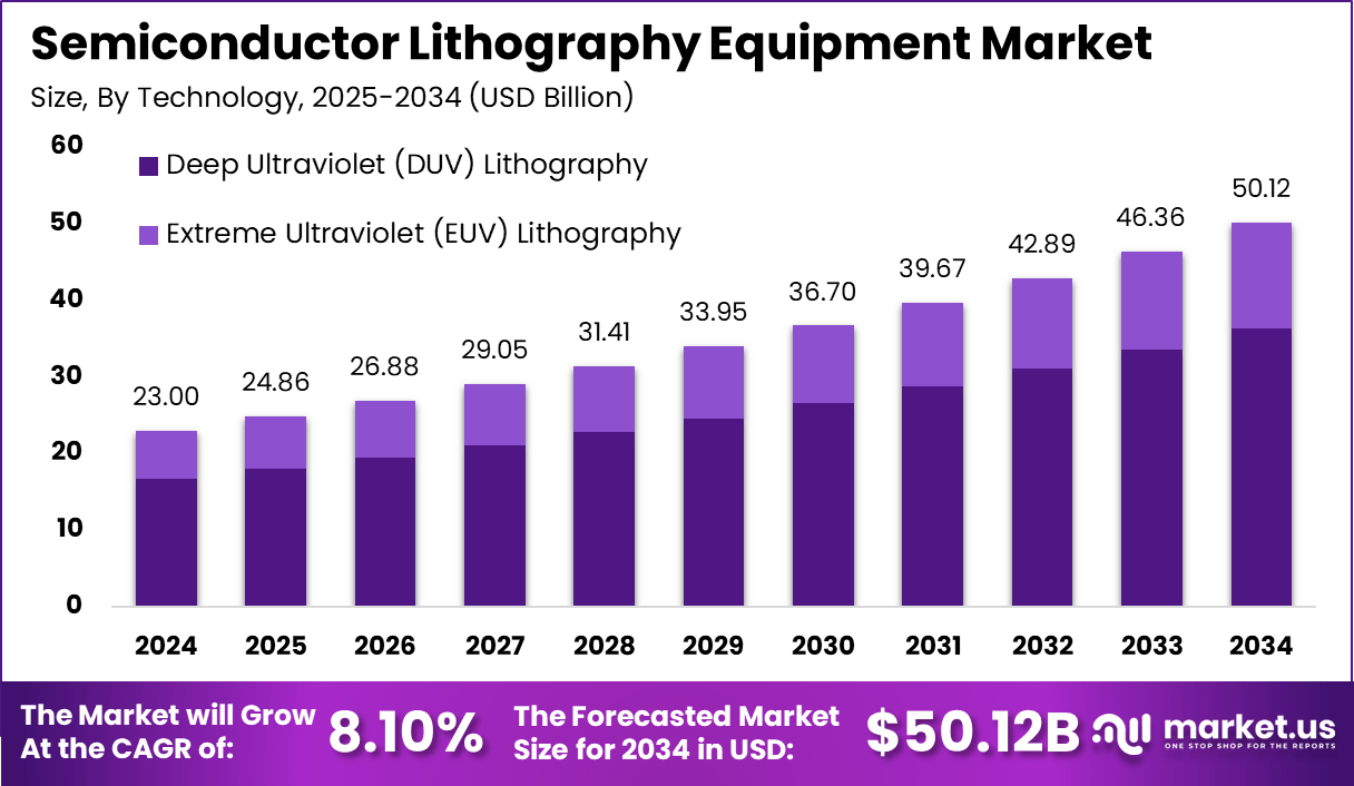
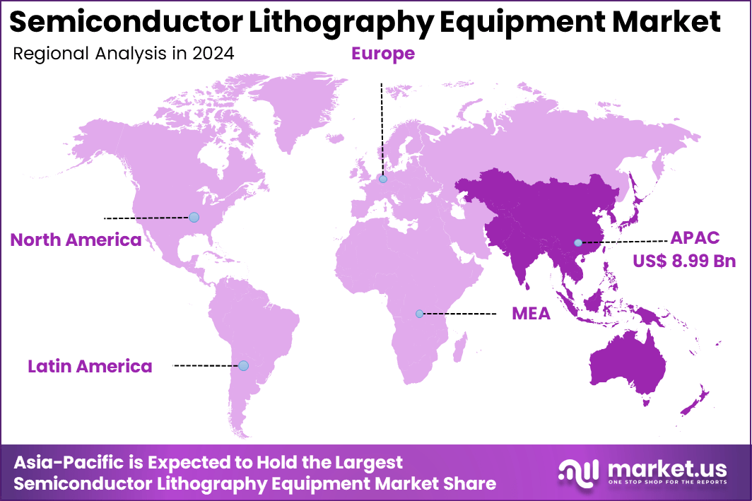
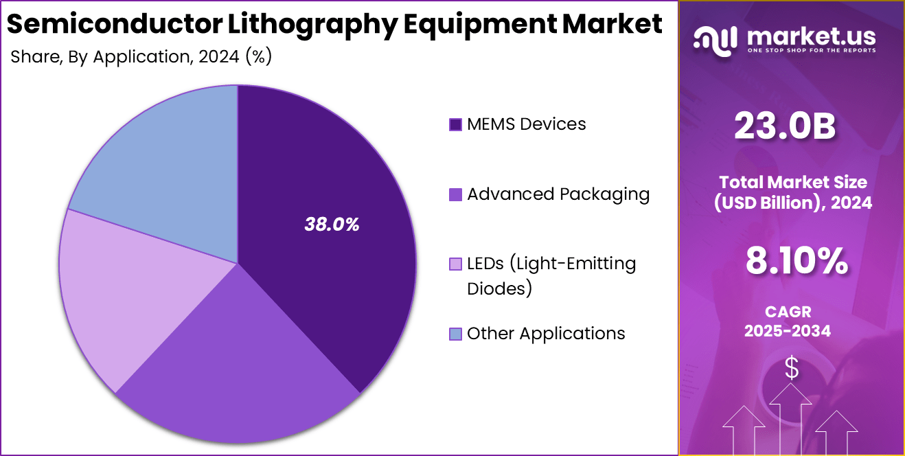
The Global Semiconductor Lithography Equipment Market is expected to be worth around USD 50.12 Billion by 2034, up from USD 23.0 Billion in 2024. It is expected to grow at a CAGR of 8.10% from 2025 to 2034. In 2024, Asia-Pacific held a dominant market position, capturing over a 39.1% share and earning USD 8.99 Billion in revenue.
The Semiconductor Lithography Equipment Market plays a critical role in the semiconductor manufacturing process, enabling the precise patterning of semiconductor materials on wafers. Lithography is a key step in producing integrated circuits (ICs) that power modern electronic devices. As semiconductor devices continue to become smaller and more powerful, lithography equipment is essential for achieving high-resolution patterns at the nanoscale.
This market includes equipment such as photolithography systems, extreme ultraviolet (EUV) lithography machines, and mask aligners, each serving a unique role in the production of microchips for various applications, from consumer electronics to automotive and industrial systems. As semiconductor technology evolves, the market for lithography equipment is poised to grow significantly, driven by advancements in manufacturing processes and the need for cutting-edge equipment to meet the demands of smaller, faster, and more efficient devices.
The growth of the semiconductor lithography equipment market is primarily driven by advancements in semiconductor technology and the increasing demand for smaller and more powerful chips. As industries such as 5G, AI, IoT, and automotive electronics require more sophisticated semiconductor components, the need for high-precision lithography systems has surged.
In particular, the move towards sub-5nm nodes for semiconductor manufacturing requires the use of extreme ultraviolet (EUV) lithography, a technology capable of creating smaller features on wafers to keep up with demand. The increasing application of advanced chips in sectors like smartphones, data centers, and automotive electronics is further driving the market’s growth.
Key Takeaways
- 2024 Market Value: The Semiconductor Lithography Equipment market is expected to be valued at USD 23.0 Billion in 2024.
- Projected Market Value: The market is projected to grow to USD 50.12 Billion by 2034, reflecting significant growth.
- CAGR: The market is expected to grow at a CAGR of 8.10% from 2025 to 2034.
- By Technology: Deep Ultraviolet (DUV) Lithography holds a dominant share of 72.5%, highlighting its essential role in semiconductor manufacturing processes.
- By Application: MEMS Devices represent 38.0% of the market, reflecting the growing demand for micro-electromechanical systems in various industries.
- Regional Insights: Asia-Pacific dominates the market with 39.1% of the market share, driven by leading semiconductor manufacturing hubs like Taiwan, South Korea, and China.
Analyst’s Review
The demand for semiconductor lithography equipment is closely tied to the increasing complexity and miniaturization of semiconductor devices. In 2024, Asia-Pacific holds a dominant position in the market, accounting for over 39.1% of the global share and earning USD 8.99 billion in revenue.
This dominance can be attributed to the presence of leading semiconductor manufacturers in countries like Taiwan, South Korea, and China. The EUV lithography segment, in particular, is experiencing rapid growth, driven by its essential role in fabricating advanced nodes, which are crucial for manufacturing the next generation of semiconductors.
As the global demand for high-performance chips increases across various industries, especially with the advent of 5G networks and the ongoing development of AI and autonomous vehicles, semiconductor manufacturers are investing heavily in advanced lithography technologies to meet these demands. The growing focus on high-performance computing and data storage solutions is also contributing to the rising need for more sophisticated lithography equipment.
The semiconductor lithography equipment market presents several growth opportunities, particularly in the EUV lithography segment. As semiconductor manufacturers continue to push the boundaries of chip miniaturization, the demand for EUV machines, which allow for the creation of intricate patterns at the 7nm and 5nm process nodes, is expected to rise significantly. The global shift towards 5G technology, quantum computing, and edge computing creates additional demand for advanced chips that require more complex manufacturing processes.
Technological advancements are at the heart of the semiconductor lithography equipment market. The transition from deep ultraviolet (DUV) lithography to extreme ultraviolet (EUV) lithography is one of the most significant developments.
EUV lithography uses 13.5nm wavelength light to create smaller and more precise patterns on semiconductor wafers, making it essential for the next-generation semiconductor nodes (5nm and below). This technology is expected to be a key enabler for manufacturing advanced microchips for emerging applications like AI, 5G, and autonomous driving.
Key Statistics
Production and Usage
- Steps in Production: Approximately 1,400 distinct steps are involved in the complete production and inspection of semiconductor wafers.
- Cost Contribution: Lithography equipment constitutes more than 50% of semiconductor fabrication costs.
- Average Production Time: A typical semiconductor fabrication process can take around 6 to 8 weeks.
- Yield Rate: The yield rate for complex semiconductor manufacturing processes can be as low as 50%.
Users
- Number of Major Semiconductor Manufacturers: Over 20 globally recognized companies.
- Number of Fabrication Facilities: Over 200 worldwide.
Application Segments
- MEMS Devices Market Share (2024): Approximately 55% of the market.
- Advanced Packaging Growth Rate (2024-2029): Approximately 9%.
- Number of MEMS Devices Produced Annually: Over 10 billion units.
Regional Analysis
In 2024, Asia-Pacific held a dominant market position in the Semiconductor Lithography Equipment Market, capturing more than 39.1% of the global share, equating to USD 8.99 billion in revenue. This dominance can be attributed to the region’s role as the global hub for semiconductor manufacturing, with key players such as Taiwan Semiconductor Manufacturing Company (TSMC), Samsung, and Intel driving the demand for advanced lithography systems.
Countries like South Korea, China, and Taiwan have substantial semiconductor fabrication plants (fabs), which are continuously upgrading to advanced nodes such as 7nm and 5nm, requiring sophisticated lithography technology to meet production standards.
The Asia-Pacific region benefits from robust government support and substantial investments in semiconductor R&D, with nations like China ramping up their domestic semiconductor manufacturing capabilities.
This is further boosted by significant manufacturing infrastructure and the concentration of high-tech industries such as consumer electronics, automotive, and communications within the region. As semiconductor demand continues to grow across industries such as 5G, AI, and IoT, Asia-Pacific’s market share in semiconductor lithography equipment is expected to remain strong.
Moreover, Asia-Pacific is at the forefront of adopting extreme ultraviolet (EUV) lithography, which is crucial for manufacturing the latest generation of microchips. The growing trend of chip miniaturization and advanced packaging in the region makes it an ideal market for high-precision lithography tools. As semiconductor technology continues to evolve, Asia-Pacific is expected to maintain its leadership in the market, driven by ongoing technological advancements and increasing demand for advanced chips.
Key Regions and Countries
- North America
- US
- Canada
- Europe
- Germany
- France
- The UK
- Spain
- Italy
- Russia
- Netherlands
- Rest of Europe
- Asia Pacific
- China
- Japan
- South Korea
- India
- Australia
- Singapore
- Thailand
- Vietnam
- Rest of APAC
- Latin America
- Brazil
- Mexico
- Rest of Latin America
- Middle East & Africa
- South Africa
- Saudi Arabia
- UAE
- Rest of MEA
By Technology
In 2024, the Deep Ultraviolet (DUV) Lithography segment held a dominant market position, capturing more than 72.5% of the global semiconductor lithography equipment market. This dominance is driven by the widespread use of DUV lithography in semiconductor fabrication, particularly for advanced process nodes above 7nm, which still represent a significant portion of semiconductor manufacturing today. DUV lithography has been the backbone of semiconductor production for years due to its reliability, proven performance, and cost-effectiveness.
Despite the growth of Extreme Ultraviolet (EUV) Lithography, DUV remains the dominant technology due to its ability to efficiently handle a wide range of applications in semiconductor manufacturing, from memory chips to microprocessor fabrication.
Its technology is mature and optimized for high-volume production, making it the go-to solution for manufacturers that are not yet focused on cutting-edge nodes like 5nm and 3nm. As semiconductor companies continue to use DUV in conjunction with multi-patterning techniques, it remains an essential part of the industry, supporting the production of a variety of chips across multiple sectors including consumer electronics, automotive, and data centers.
By Application
In 2024, the MEMS Devices segment held a dominant market position, capturing more than 38.0% of the global semiconductor lithography equipment market. This leadership is driven by the growing demand for micro-electromechanical systems (MEMS), which are used in a wide variety of applications, including sensors, actuators, and microprocessors. MEMS devices are crucial for enabling advanced technologies in industries like automotive, consumer electronics, healthcare, and consumer appliances.
The demand for MEMS devices is expanding as these systems become essential components in smartphones, wearable technology, and automotive safety systems, which require highly accurate and miniature devices. MEMS production requires precise lithography techniques, and semiconductor lithography equipment plays a key role in ensuring the high-quality manufacturing of these miniaturized devices.
As MEMS technology advances, particularly in the development of MEMS sensors for IoT applications and autonomous vehicles, the need for reliable and high-precision lithography equipment will only increase. The scalability and cost-effectiveness of MEMS production further cement its position as the leading application in the semiconductor lithography equipment market. As these devices become more integral to future technologies, MEMS will continue to drive significant growth in the market.
Key Market Segments
By Technology
- Deep Ultraviolet (DUV) Lithography
- Extreme Ultraviolet (EUV) Lithography
By Application
- Advanced Packaging
- MEMS Devices
- LEDs (Light-Emitting Diodes)
- Other Applications
Driving Factors
Increasing Demand for Advanced Semiconductors
The increasing demand for advanced semiconductors is one of the major driving factors for the growth of the Semiconductor Lithography Equipment Market. As the world becomes more reliant on smart devices, 5G technology, AI, and IoT, the need for smaller, faster, and more powerful semiconductors continues to grow.
This surge in demand for advanced chips is pushing manufacturers to upgrade their fabrication technologies, requiring the latest lithography equipment. Semiconductor devices are constantly evolving, and as industries like automotive, consumer electronics, and healthcare demand more sophisticated chips, the need for precise and efficient lithography techniques becomes more urgent.
Advanced lithography technologies, such as Extreme Ultraviolet (EUV) lithography, are becoming more critical to meet the demand for smaller process nodes in semiconductor manufacturing, particularly for 5nm and 3nm chips.
With these advancements, the semiconductor industry is pushing the boundaries of miniaturization, where even the smallest defects in wafers can cause significant issues in device performance. The adoption of DUV and EUV lithography equipment is, therefore, essential for achieving high yields and quality in semiconductor production. As demand for cutting-edge chips continues to rise, semiconductor lithography equipment will play an increasingly important role in meeting these technological needs.
Restraining Factors
High Cost of Lithography Equipment
One of the key restraining factors in the Semiconductor Lithography Equipment Market is the high cost of advanced lithography systems, particularly Extreme Ultraviolet (EUV) lithography machines. EUV technology is essential for producing chips at smaller nodes (such as 5nm and 3nm), but it comes with an enormous price tag, often exceeding hundreds of millions of dollars per machine.
This significant upfront investment makes it difficult for smaller semiconductor manufacturers and companies in emerging markets to afford the latest equipment. The ongoing operational costs, including the need for specialized maintenance, frequent upgrades, and trained personnel, further increase the financial burden.
Moreover, the high cost of lithography equipment limits its adoption to major semiconductor players like Intel, TSMC, and Samsung, creating a barrier for smaller firms or those with limited budgets. This price disparity can contribute to market consolidation, where larger companies continue to dominate the market while smaller players struggle to keep up.
Although technological advancements are gradually lowering costs, the initial expense and ongoing maintenance costs associated with high-end lithography systems remain a significant hurdle for the market’s broader expansion, especially in developing regions.
Growth Opportunities
Expansion in Emerging Markets
A significant growth opportunity in the Semiconductor Lithography Equipment Market lies in the expansion of semiconductor production in emerging markets, particularly in Asia-Pacific, India, and Latin America. As countries like China and India invest heavily in developing their domestic semiconductor manufacturing capabilities, there is a growing demand for state-of-the-art lithography equipment.
This trend is driven by government initiatives aimed at reducing dependence on imports and fostering local innovation in advanced technologies. For instance, China’s push to boost its semiconductor industry through government support and investment in research and development is opening up substantial opportunities for lithography equipment suppliers.
Additionally, the increasing demand for consumer electronics and automotive electronics in these regions is driving the need for more sophisticated semiconductor components. As these markets mature, local companies are increasingly adopting advanced lithography systems to meet the rising demand for high-performance chips. Manufacturers that offer cost-effective, high-precision lithography solutions will find great success in catering to these emerging markets, contributing to the overall growth of the global semiconductor lithography equipment market.
Challenging Factors
Technological Complexity and Advancements
A significant challenging factor in the Semiconductor Lithography Equipment Market is the increasing technological complexity of modern semiconductor fabrication. As semiconductor nodes continue to shrink, the need for increasingly advanced lithography systems becomes more critical. Technologies like EUV and multi-patterning demand high precision and complex manufacturing processes, requiring lithography systems to be constantly upgraded and innovated. These developments are often highly challenging and require significant expertise, pushing the boundaries of existing technology.
Moreover, the continual drive for smaller and more powerful semiconductor devices is creating a mismatch between the capabilities of current lithography equipment and the requirements of next-generation chips. For example, creating 3D chips and advanced packaging technologies requires new lithography approaches and techniques, such as mask-free lithography and nano-imprint lithography, which are still in their developmental stages.
This technological race creates significant challenges for equipment manufacturers, as they must continuously innovate to keep up with the demands of an ever-evolving market. The pressure to meet these demands while maintaining cost-efficiency, high throughput, and low defect rates is a substantial challenge, affecting the market’s overall growth and development.
Growth Factors
Rising Demand for Advanced Chip Technology
The demand for advanced semiconductor chips continues to be a major growth driver for the Semiconductor Lithography Equipment Market. As industries such as 5G, AI, automotive electronics, and IoT expand, the need for high-performance semiconductors is growing rapidly.
According to market research, the global semiconductor market is expected to reach USD 1 trillion by 2030, which directly impacts the demand for lithography equipment. As chips become more powerful and smaller, semiconductor manufacturers are investing heavily in advanced lithography technologies to keep pace with this growing demand.
Emerging Trends
Integration of AI and Automation in Lithography
One of the most notable emerging trends in the Semiconductor Lithography Equipment Market is the increasing integration of AI and automation. As the industry faces the challenges of miniaturizing semiconductor components further, the role of artificial intelligence in improving lithography systems has become more pronounced.
AI enables predictive maintenance, improving system uptime, and reducing downtime, which is crucial for high-volume production in semiconductor fabs. This trend is not only reducing operational costs but also enhancing the precision of lithography machines.
Business Benefits
Enhanced Yield and Cost Efficiency
Investing in advanced semiconductor lithography equipment brings significant business benefits, especially in terms of enhanced yield and cost efficiency. As semiconductor manufacturers are increasingly required to produce chips with smaller nodes and more intricate designs, the role of lithography equipment in ensuring high-quality and defect-free wafers becomes even more crucial.
High-end lithography systems, particularly EUV, provide high resolution and accuracy, which ultimately lead to higher yield rates. Companies using EUV lithography have seen a reduction in wafer defects, leading to a more cost-effective production process.
Business Opportunities
Expansion of Semiconductor Manufacturing in Emerging Markets
A significant business opportunity in the Semiconductor Lithography Equipment Market lies in the expansion of semiconductor manufacturing in emerging markets, particularly in regions like Asia-Pacific, India, and Latin America.
The growing semiconductor production in these regions is driven by government initiatives aimed at building self-sufficient supply chains and reducing dependence on imports. China alone is expected to invest USD 150 billion into its semiconductor industry by 2030, boosting demand for advanced lithography equipment.
Key Players Analysis
ASML Holding N.V. is the undisputed leader in the Semiconductor Lithography Equipment Market, particularly in the development of Extreme Ultraviolet (EUV) lithography systems. As of 2024, ASML remains the only company capable of producing EUV lithography machines, which are essential for manufacturing 5nm and 3nm semiconductor nodes.
Nikon Corporation is another key player in the semiconductor lithography equipment market, known for its high-precision Deep Ultraviolet (DUV) lithography systems. Nikon’s main strength lies in its ability to produce cost-effective, reliable DUV lithography machines used for manufacturing at larger nodes (above 7nm). While ASML has dominated the EUV segment, Nikon has carved out a substantial presence with DUV systems, especially in mid-range node fabrication.
Canon Inc. is another significant player in the semiconductor lithography equipment market, especially in DUV and mask aligner systems. Canon’s lithography machines are primarily used for low-to-mid-volume production of semiconductors and optical devices. While Canon has not yet made a significant push into the EUV market, it remains competitive by offering cost-effective solutions for high-precision lithography in the 5G and automotive semiconductor sectors.
Top Key Players in the Market
- ASML Holding N.V.
- Nikon Corporation
- Canon Inc.
- Veeco Instruments Inc.
- EV Group
- SUSS MicroTec SE
- JEOL Ltd.
- Onto Innovation Inc.
- Other Key Players
Recent Developments
- In 2024, ASML introduced an upgraded EUV lithography system, designed to improve throughput and precision for sub-5nm semiconductor nodes, meeting the growing demand for advanced chips.
- In 2024, Nikon launched its new DUV lithography machine, offering enhanced resolution capabilities to support next-generation chip production at 7nm and above process nodes.
Report Scope
| Report Features | Description |
|---|---|
| Market Value (2024) | USD 23.0 Billion |
| Forecast Revenue (2034) | USD 50.12 Billion |
| CAGR (2025-2034) | 8.10% |
| Largest Market | North America |
| Base Year for Estimation | 2024 |
| Historic Period | 2020-2023 |
| Forecast Period | 2025-2034 |
| Report Coverage | Revenue Forecast, Market Dynamics, Competitive Landscape, Recent Developments |
| Segments Covered | By Technology (Deep Ultraviolet (DUV) Lithography, Extreme Ultraviolet (EUV) Lithography), By Application (Advanced Packaging, MEMS Devices, LEDs (Light-Emitting Diodes), Other Applications) |
| Regional Analysis | North America (US, Canada), Europe (Germany, UK, Spain, Austria, Rest of Europe), Asia-Pacific (China, Japan, South Korea, India, Australia, Thailand, Rest of Asia-Pacific), Latin America (Brazil), Middle East & Africa(South Africa, Saudi Arabia, United Arab Emirates) |
| Competitive Landscape | ASML Holding N.V., Nikon Corporation, Canon Inc., Veeco Instruments Inc., EV Group, SUSS MicroTec SE, JEOL Ltd., Onto Innovation Inc., Other Key Players |
| Customization Scope | We will provide customization for segments and at the region/country level. Moreover, additional customization can be done based on the requirements. |
| Purchase Options | We have three licenses to opt for Single User License, Multi-User License (Up to 5 Users), Corporate Use License (Unlimited User and Printable PDF) |


