
Quick Navigation
Report Overview
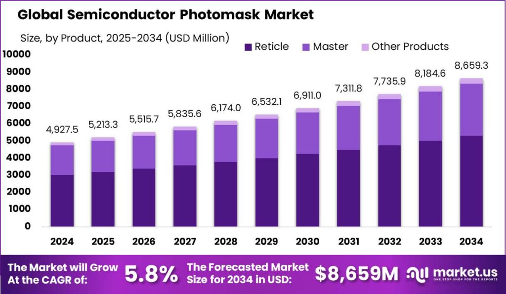
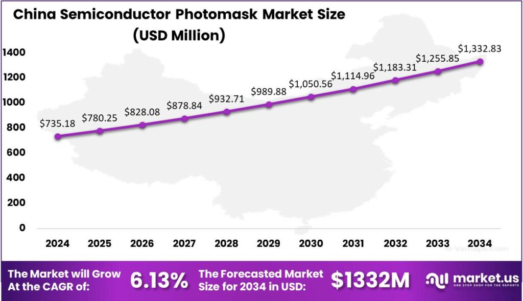
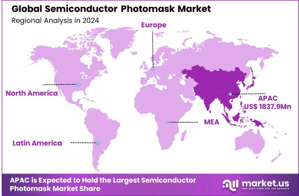
The Global Semiconductor Photomask Market size is expected to be worth around USD 8,659 Mn By 2034, from USD 4927.5 Mn in 2024, growing at a CAGR of 5.80% during the forecast period from 2025 to 2034. In 2024, Asia-Pacific (APAC) held over 37.3% of the global semiconductor photomask market, contributing approximately USD 1,837.9 Million in revenue. The China market is projected to reach USD 735.18 Mn with a CAGR of 6.13%.
A semiconductor photomask is a key component used in the photolithography process of semiconductor manufacturing. A photomask is a high-precision glass or quartz plate, typically coated with chrome, that serves as a template for transferring detailed circuit patterns onto semiconductor wafers during photolithography. The precision and quality of photomasks are critical to the performance and reliability of semiconductor products, making them essential in semiconductor manufacturing.
The semiconductor photomask market is driven by the growing demand for advanced electronic devices like smartphones, tablets, and high-performance computing systems. As semiconductor technologies evolve, with a focus on smaller geometries and transitions to 5nm and 3nm nodes, the need for photomasks with higher resolution and precision increases.
The market is further boosted by the rise of AI, IoT, and autonomous vehicles, which demand more efficient semiconductors. The push for next-gen technologies like 5G drives innovation in semiconductor processes. Additionally, increased investments in semiconductor fabs, especially in Asia-Pacific and North America, contribute to market growth.
According to SEMI’s Electronics System Design Alliance (ESDA), there have been notable double-digit increases in key areas of EDA, such as reticle enhancement technology (RET) and mask data preparation (MDP). Specifically, RET has grown by 21.3%, while MDP surged by 17.3% over the rolling four quarters through the first quarter of 2024.
Based on data from SEMI’s 2023 Photomask Characterization Report, The semiconductor photomask market demonstrated strong performance in 2023, generating $5.4 billion in revenue. This growth is part of a larger trend across the semiconductor ecosystem, with adjacent sectors like electronic design automation (EDA) also seeing significant expansion.
A key trend in the semiconductor photomask industry is the rising demand for extreme ultraviolet (EUV) lithography. As chip manufacturers move to smaller process nodes, EUV enables more precise patterning. Additionally, the growth of 3D chip architectures and advanced packaging techniques presents new challenges and opportunities for photomask manufacturers to innovate in design and production.
Technological advancements, such as multi-patterning and maskless lithography, are transforming the photomask industry. Multi-patterning allows manufacturers to improve resolution without overhauling existing equipment. Meanwhile, maskless lithography, still in development, could eliminate the need for physical masks, enabling faster and more flexible production.
Key Takeaways
- The Global Semiconductor Photomask Market size is expected to reach USD 8,659 million by 2034, growing from USD 4,927.5 million in 2024, at a compound annual growth rate (CAGR) of 5.80% during the forecast period from 2025 to 2034.
- In 2024, the Reticle segment dominated the semiconductor photomask market, capturing over 61.3% of the global market share.
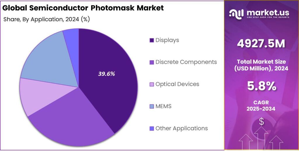
- The Displays segment held a dominant market position in 2024, with more than a 39.6% share of the semiconductor photomask market.
- Asia-Pacific (APAC) accounted for a significant portion of the semiconductor photomask market in 2024, holding over 37.3% of the global market share, contributing approximately USD 1.84 Million in revenue.
- The semiconductor photomask market in China is projected to reach a valuation of USD 735.18 million by 2024, with a CAGR of 6.13%.
China Market Size
The semiconductor photomask market in China is projected to reach a valuation of USD 735.18 million by the year 2024, reflecting a compound annual growth rate (CAGR) of 6.13%. This steady growth indicates a robust demand for photomasks, which are integral to the semiconductor manufacturing process.
This growth is driven by several factors, including advancements in semiconductor technology. Applications in emerging fields like artificial intelligence (AI), 5G communications, and automotive electronics are increasing the demand for more sophisticated chips. These technologies require finer and more precise lithographic patterns, which in turn raises the need for high-performance photomasks.
Additionally, China’s focus on becoming self-reliant in semiconductor manufacturing, coupled with the development of domestic semiconductor foundries, is likely to bolster the demand for photomasks. As Chinese semiconductor companies expand production, the demand for photomasks to support advanced fabrication processes will increase.
In 2024, Asia-Pacific (APAC) held a dominant market position in the semiconductor photomask sector, capturing over 37.3% of the global market share, with a revenue contribution of approximately USD 1.84 billion. This leadership can be attributed to the region’s stronghold in semiconductor manufacturing, particularly in countries like China, South Korea, Japan, and Taiwan.
Asia-Pacific is home to some of the largest semiconductor foundries in the world, such as TSMC (Taiwan Semiconductor Manufacturing Company) and Samsung Electronics, both of which are major consumers of photomasks. The region’s rapid technological advancements, coupled with the scaling of semiconductor production to meet the demands of emerging technologies like AI, 5G, and IoT, further solidify its dominance.
China plays a crucial role in the semiconductor photomask market. The country has been heavily investing in its semiconductor industry to reduce dependency on foreign technology and develop a more self-sufficient supply chain. This has led to an increased demand for advanced photomasks to support the production of cutting-edge chips.
North America and Europe have smaller shares of the semiconductor photomask market. The U.S. industry grows due to rising demand in automotive electronics and data centers, while Europe remains smaller but invests in advanced technologies for specialized fields like aerospace and defense.
Product Analysis
In 2024, the Reticle segment dominated the semiconductor photomask market, capturing over 61.3% of the global market share. The dominance of the Reticle segment can be attributed to its critical role in the photolithography process, where it is used to define the circuit patterns on semiconductor wafers.
Reticles are essential for the production of high-precision semiconductor devices, and as the demand for advanced integrated circuits (ICs) in applications like 5G, AI, and automotive electronics continues to rise, the need for high-quality reticles has surged. The superior resolution and precision offered by reticles make them indispensable in the manufacturing of state-of-the-art microchips.
Reticles are used extensively in the production of advanced node semiconductors, such as those built on 7nm, 5nm, and even smaller processes. This has been a driving factor behind their market dominance, as the semiconductor industry increasingly focuses on smaller, more efficient chips with greater processing power.
As semiconductor miniaturization advances, the demand for precise reticles grows. Smaller chips require more complex patterns, driving the need for high-precision photomasks. Semiconductor foundries are investing in advanced photomask technologies to support cutting-edge manufacturing, ensuring continued growth in the Reticle segment.
Application Analysis
In 2024, the Displays segment held a dominant market position, capturing more than a 39.6% share of the semiconductor photomask market. This dominance can be attributed to the rapid advancements in display technologies, especially in the production of OLED and LCD panels.
As demand for high-quality displays increases across smartphones, televisions, and digital signage, manufacturers are requiring photomasks with higher precision and finer resolutions to meet stringent display resolution requirements. The continuous push for sharper, more vibrant displays in consumer electronics has thus contributed significantly to the growth of this segment.
The Discrete Components segment plays a key role but has a smaller market share. While photomasks are essential for components like diodes and resistors, demand grows slower than in displays. This is due to reliance on established processes, leading to slower innovation in photomask technology compared to sectors like displays or MEMS.
In the Optical Devices segment, photomasks are crucial for producing lenses, sensors, and mirrors. While demand grows in automotive and healthcare sectors, it remains lower than in displays. The segment is steadily growing due to advancements in optical technologies but does not yet match the market share or growth potential of displays.
Key Market Segments
By Product
- Reticle
- Master
- Other Products
By Application
- Displays
- Discrete Components
- Optical Devices
- MEMS
- Other Applications
Key Regions and Countries
- North America
- US
- Canada
- Europe
- Germany
- France
- The UK
- Spain
- Italy
- Rest of Europe
- Asia Pacific
- China
- Japan
- South Korea
- India
- Australia
- Singapore
- Rest of Asia Pacific
- Latin America
- Brazil
- Mexico
- Rest of Latin America
- Middle East & Africa
- South Africa
- Saudi Arabia
- UAE
- Rest of MEA
Driver
Increasing Demand for Advanced Electronics
The demand for advanced semiconductor technologies, particularly in consumer electronics, automotive, and telecommunications, is a significant driver for the photomask market. As electronic devices become more sophisticated, the need for smaller, faster, and more efficient components has grown exponentially. Semiconductor photomasks are essential in photolithography, where they play a crucial role in patterning microcircuits onto silicon wafers.
The growing adoption of 5G technology, electric vehicles (EVs), and AI-based systems all require cutting-edge semiconductor chips with finer features and high-performance capabilities. This has accelerated the need for photomasks that can support the production of these advanced chips. With the continuous trend of miniaturization in semiconductor manufacturing, photomasks are critical to achieving higher precision and performance in modern electronic products.
Restraint
High Manufacturing Costs
A major restraint in the semiconductor photomask market is the high cost of photomask manufacturing, which can be prohibitive, especially for small and medium-scale manufacturers. The photomask production process involves sophisticated equipment, highly skilled labor, and stringent quality control standards. The cost of producing photomasks increases with the complexity of the semiconductor designs, particularly as the demand for smaller nodes in semiconductor chips rises.
As semiconductor devices continue to scale down to nanometer levels, the intricacies of photomask design become more complex, demanding higher precision in fabrication. This inevitably leads to escalating costs, both in terms of technology investments and operational expenditures. Additionally, the maintenance and updating of photomask production facilities, as well as the integration of advanced materials like glass and quartz, further elevate overall costs.
Opportunity
Emerging Markets in Asia-Pacific
The Asia-Pacific region presents a significant opportunity for growth in the semiconductor photomask market. As a hub for semiconductor manufacturing, countries such as China, South Korea, Japan, and Taiwan are continuously ramping up their production capacities to meet the growing global demand for advanced semiconductor components.
China, in particular, is heavily investing in its semiconductor industry, with the aim of reducing its dependence on foreign suppliers. The Chinese government’s push for technological self-sufficiency is creating ample opportunities for local semiconductor photomask suppliers to capture market share. Furthermore, the rise of emerging technologies such as 5G, IoT, and artificial intelligence is creating new avenues for photomask manufacturers to provide tailored solutions for increasingly complex chip designs.
Challenge
Shortage of Skilled Labor
A critical challenge faced by the semiconductor photomask industry is the shortage of skilled labor. The photomask production process is highly specialized and requires professionals with expertise in lithography, optics, and material science. However, there is a growing gap between the demand for these specialized skills and the available workforce.
As semiconductor technologies evolve, the intricacies of photomask design and production become more complex, requiring a deeper understanding of advanced manufacturing techniques. Many semiconductor manufacturing hubs, especially in emerging markets, are struggling to recruit and retain professionals with the necessary skill set. This shortage is particularly evident in regions where the semiconductor industry is growing rapidly, but education and training infrastructure for these high-tech roles is lagging behind.
Emerging Trends
A key trend in this sector is the continuous push towards smaller nodes in semiconductor manufacturing. As the demand for smaller, more efficient chips grows, the photomask technology must evolve to keep pace. EUV photomasks are essential for the fabrication of semiconductor devices at nodes smaller than 7 nm, and their adoption is expected to continue growing.
Another significant trend is the rise of multi-patterning techniques, which are used to overcome the limitations of optical lithography. These techniques use multiple exposure steps to create finer patterns on photomasks, meeting the demand for smaller transistors. The growing use of advanced materials like PSM and APSM enhances photomask resolution, allowing for more intricate semiconductor structures.
The market is seeing more investments in automating and digitizing photomask production, improving efficiency, reducing defects, and ensuring consistency. Innovations in mask inspection, such as AI and machine learning, are enhancing defect detection, leading to more precise, efficient, and scalable semiconductor photomasks.
Business Benefits
One of the primary advantages is that they enable the production of highly precise semiconductor devices. By utilizing advanced photomask technology, companies can produce chips with smaller nodes, higher processing power, and lower energy consumption. These improvements in chip performance align with the rising global demand for faster and more energy-efficient consumer electronics, driving revenue growth for manufacturers.
Moreover, the development of photomasks using EUV lithography allows companies to manufacture advanced chips at scale, which is vital for industries such as artificial intelligence (AI), automotive electronics, and telecommunications. By leveraging advanced photomasks, companies can tap into these growing markets and remain competitive.
Investing in high-quality photomasks also translates to reduced production costs in the long run. With the introduction of automation in the photomask manufacturing process, companies can improve operational efficiency, reduce waste, and shorten production cycles. This reduction in manufacturing costs leads to better profit margins for businesses.
Key Player Analysis
Advance Reproductions Corp. is a prominent player in the semiconductor photomask industry, providing high-quality photomask services. They are known for their focus on precision and advanced technology, catering to both large-scale semiconductor manufacturers and smaller, specialized operations.
Applied Materials Inc. is one of the global leaders in materials engineering, with a strong presence in the semiconductor photomask market. The company provides advanced equipment and services used in the production of photomasks. Applied Materials is particularly recognized for its technological innovation in photomask inspection and repair services.
HOYA Corporation, a Japanese multinational, is a key player in the photomask market, known for its high-quality photomask production. HOYA specializes in delivering highly precise photomasks for advanced semiconductor applications, including photolithography processes. With decades of expertise and a commitment to research and development, HOYA stands as a top choice for manufacturers needing ultra-precise photomasks.
Top Key Players in the Market
- Advance Reproductions Corp.
- Applied Materials Inc.
- HOYA Corporation
- Infinite Graphics Incorporated
- KLA Corporation
- LG Innotek Co. Ltd
- Toppan Photomasks; Inc.
- Nippon Filcon Co. Ltd.
- Photronics Inc.
- SK-Electronics Co. Ltd.
- Other Major Players
Top Opportunities Awaiting for Players
The semiconductor photomask market is set for significant growth, with key opportunities emerging for players in the industry.
- Rising Demand for Advanced Semiconductor Nodes: As technology advances, the demand for smaller, more powerful semiconductors increases. This drives the need for higher precision photomasks, especially in nodes below 7nm. Companies that can provide these advanced photomask solutions will be in high demand.
- Growth in 5G and AI Technologies: The expansion of 5G networks and the rise of artificial intelligence are creating a surge in semiconductor production. Photomask manufacturers have the opportunity to support these sectors by providing high-quality masks for more complex chip designs.
- Increased Focus on EVs and Autonomous Vehicles: With the growing popularity of electric vehicles (EVs) and autonomous driving technologies, the need for semiconductors in these applications is also rising. Photomask companies can tap into this by providing customized solutions for automotive chips.
- Investment in Next-Gen Lithography: As EUV (extreme ultraviolet) lithography becomes more prevalent, there’s a need for photomasks capable of meeting the stringent requirements of this technology. Early movers in this area can secure a leading position in the market.
- Regional Expansion: With semiconductor production ramping up in regions like Asia and North America, photomask manufacturers have an opportunity to expand their footprint and establish local partnerships, optimizing supply chains and cutting down on lead times.
Recent Developments
- In February 2024, Toppan Photomasks, Inc. and IBM have formed a joint R&D partnership focused on advancing EUV semiconductor photomasks. By leveraging their combined expertise in materials and process control, the collaboration aims to deliver innovative solutions for 2nm node and beyond printing.
- In July 2024, Acrotec Group, based in Switzerland, acquired Lasertec B.V. from the Netherlands. Lasertec, known for its expertise in laser photomask inspection systems, will help Acrotec enhance its precision machining and laser cutting capabilities, solidifying its position in the photomask market. This acquisition underscores the growing demand for high-precision equipment in semiconductor manufacturing.
- Meanwhile, in December 2023, Dai Nippon Printing Co., Ltd. (DNP), based in Tokyo, made a significant breakthrough by successfully developing a photomask fabrication process capable of supporting a 3-nanometer (10-9 meter) lithography process. This advanced technique is tailored for extreme ultraviolet (EUV) lithography, a cutting-edge technology used in state-of-the-art semiconductor manufacturing.
Report Scope
| Report Features | Description |
|---|---|
| Market Value (2024) | USD 4,927.5 Mn |
| Forecast Revenue (2034) | USD 8,659 Mn |
| CAGR (2025-2034) | 5.80% |
| Base Year for Estimation | 2024 |
| Historic Period | 2020-2023 |
| Forecast Period | 2025-2034 |
| Report Coverage | Revenue Forecast, Market Dynamics, COVID-19 Impact, Competitive Landscape, Recent Developments |
| Segments Covered | By Product (Reticle, Master, Other Products), By Application (Displays, Discrete Components, Optical Devices, MEMS, Other Applications) |
| Regional Analysis | North America – US, Canada; Europe – Germany, France, The UK, Spain, Italy, Russia, Netherlands, Rest of Europe; Asia Pacific – China, Japan, South Korea, India, New Zealand, Singapore, Thailand, Vietnam, Rest of APAC; Latin America – Brazil, Mexico, Rest of Latin America; Middle East & Africa – South Africa, Saudi Arabia, UAE, Rest of MEA |
| Competitive Landscape | Advance Reproductions Corp., Applied Materials Inc., HOYA Corporation, Infinite Graphics Incorporated, KLA Corporation, LG Innotek Co. Ltd, Toppan Photomasks; Inc., Nippon Filcon Co. Ltd., Photronics Inc., SK-Electronics Co. Ltd., Other Major Players |
| Customization Scope | Customization for segments, region/country-level will be provided. Moreover, additional customization can be done based on the requirements. |
| Purchase Options | We have three license to opt for: Single User License, Multi-User License (Up to 5 Users), Corporate Use License (Unlimited User and Printable PDF) |


