Report Overview
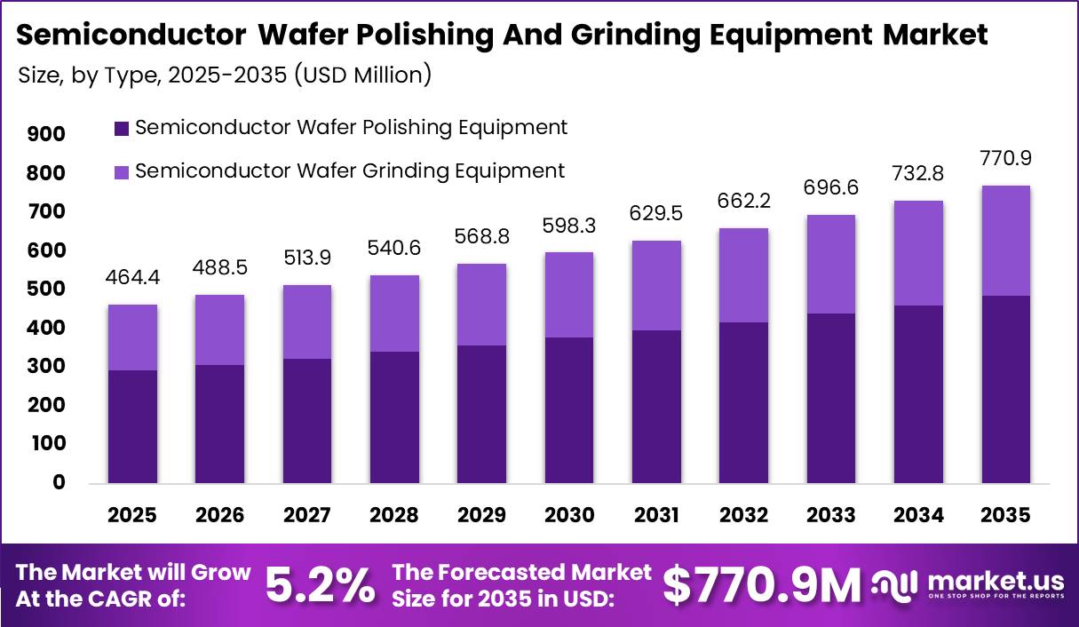
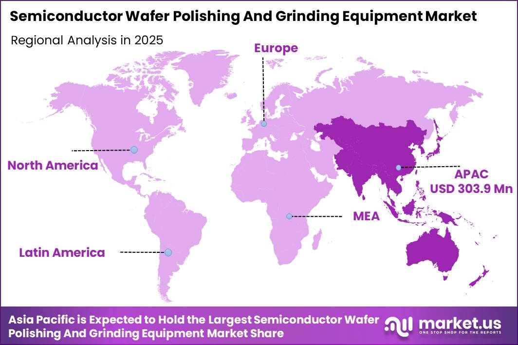
In 2025, the Global Semiconductor Wafer Polishing And Grinding Equipment Market was valued at USD 464.4 million. The market is projected to grow at a CAGR of 5.2% during 2026–2035, reaching approximately USD 770.9 million by 2035. Asia Pacific dominated the global market in 2025, accounting for more than 65.3% of the total market share and generating approximately USD 303.9 million in revenue.
The rapid expansion of global semiconductor production supports market growth. The Semiconductor Industry Association reported that worldwide chip sales reached a record USD 791.7 billion in 2025, increasing 25.6% from USD 630.5 billion in 2024, and could approach USD 1 Trillion in 2026.
Similarly, World Semiconductor Trade Statistics recorded USD 795.6 billion in semiconductor sales during 2025, representing a 26.2% increase. Higher demand from artificial intelligence systems, data centers, memory devices, and advanced processors is encouraging chipmakers to expand fabrication capacity. These investments directly increase the need for grinding and polishing equipment used to thin, flatten, and prepare silicon wafers.
Asia Pacific remained the largest regional market, contributing the highest share of overall market revenue. WSTS reported that regional semiconductor revenue reached USD 421.4 billion in 2025 and is expected to rise to USD 526.3 billion in 2026, reflecting 24.9% annual growth. In addition, global silicon wafer shipments increased 5.8% in 2025 to 12,973 Million Square Inches.
Key Takeaway
- The Semiconductor Wafer Polishing And Grinding Equipment Market was valued at USD 464.4 million in 2025, projected to reach USD 770.9 million by 2035 at a 5.2% CAGR.
- Semiconductor Wafer Polishing Equipment led the type segment with a 63.1% share.
- Advanced Nodes dominated the technology node segment with a 71.3% share.
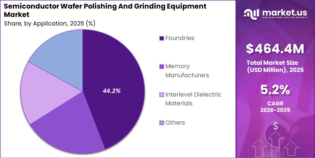
- Foundries led the application segment with a 44.2% share.
- Asia Pacific led the market with a 65.3% share, generating approximately USD 303.9 million in 2025.
Market Statistics and Data Insights
- Global wafer-fab equipment sales reached a record USD 116.9 billion in 2025 and are forecast to increase 23.1% to USD 143.9 billion in 2026. Actual worldwide semiconductor equipment billings reached USD 36.5 billion in Q1 2026, rising 14% year-over-year. Higher front-end investment directly supports the purchase of CMP, wafer thinning, back-grinding, cleaning, and surface-control systems.
- Worldwide 300 mm memory-fab equipment investment is forecast to rise 29% to USD 52 billion in 2026. Within this total, DRAM equipment spending is expected to reach USD 37 billion, while 3D NAND equipment investment is projected at USD 14 billion. Global 300 mm memory capacity is also expected to reach 4.1 million wafers per month in 2026.
- TSMC reported that 3 nm products represented 24% of its 2025 wafer revenue, while technologies at 7 nm and below accounted for 74%. The company shipped 15.0 million 12-inch-equivalent wafers in 2025, compared with 12.9 million in 2024.
- US export regulations introduced controls on 24 categories of semiconductor manufacturing equipment and 3semiconductor-development software categories. The rules also added 140 entities to the Entity List and modified 14 existing entries. These measures cover equipment, components, software, and technologies used in advanced semiconductor production.
- EBARA states that CMP equipment used on a 300 mm wafer must deliver surface-flattening accuracy within 10 nm. SEMI also reports that wafer-surface features as small as 20 nm can create post-CMP dielectric-thickness variations that may affect circuit performance and production yield.
- SK hynix began mass production of its 321-layer, 2-terabit QLC NAND product in August 2025. The design increased independently operating planes from 4 to 6, doubled data-transfer speed, improved write performance by up to 56%, raised read performance by 18%, and improved write-power efficiency by more than 23%. Such high-layer-count devices increase the importance of controlling wafer stress, thickness, bow, and warpage.
- A January 2026 US-Taiwan trade and investment agreement included commitments for Taiwanese semiconductor and technology companies to make at least USD 250 billion in new direct investment in US semiconductor, energy, and AI manufacturing capacity.
- SEMI forecast global silicon-wafer shipments to increase 5.4% to 12,824 million square inches in 2025, supported partly by polished wafers used in high-bandwidth memory. Actual Q1 2026 shipments reached 3,275 million square inches, increasing 13.1% from 2,896 million square inches in Q1 2025.
- DISCO’s 2025 DFG8561 wafer grinder delivered 1.6 times the productivity of the previous model after its wafer-transfer and cleaning mechanisms were redesigned to reduce processing time.
- A 2025 CMP study found that radial-groove polishing pads reduced experimental slurry-saturation time from 21.5 seconds to 16.06 seconds, representing an approximately 25.4% reduction compared with concentric-groove pads.
By Type
The Semiconductor Wafer Polishing Equipment segment held a leading 63.1% share, supported by its essential role in advanced chip manufacturing. Polishing is required to create the highly smooth and flat wafer surfaces needed for accurate circuit patterning.
SEMI reported that global semiconductor manufacturing equipment sales reached a record USD 135.1 billion in 2025, increasing 15% from USD 117.1 billion in 2024. This growth was driven by rising investment in advanced logic chips, memory devices, artificial intelligence infrastructure, and new fabrication capacity.
Chemical mechanical polishing helps wafers achieve nanometer-level surface accuracy before lithography and other production stages. Without proper polishing, uneven surfaces can reduce pattern accuracy, lower production yields, and increase the risk of chip defects. SEMI’s World Fab Forecast also indicated that global foundry capacity increased 10% year-on-year in 2025 and is expected to expand by another 9% in 2026.
By Technology Node
The Advanced Nodes segment held a dominant 71.3% share, supported by the rapid expansion of leading-edge semiconductor manufacturing. According to SEMI’s 300mm Fab Outlook, advanced process capacity for 7nm and below is expected to increase from 850,000 wafers per month in 2024 to nearly 1.4 million wafers per month by 2028, representing growth of about 69%.
Major chipmakers are also directing large investments toward advanced production technologies. TSMC increased its capital expenditure to USD 40.9 billion in 2025, with around 70%–80% allocated to expanding 2-nanometer and 3-nanometer manufacturing capacity. Smaller transistor sizes require extremely smooth and flat wafer surfaces because even minor irregularities can affect lithography accuracy and reduce chip yields.
As a result, advanced wafer processing requires high-precision polishing and grinding equipment. Production capacity for 2nm and below technologies is projected to rise from less than 200,000 wafers per month in 2025 to more than 500,000 wafers per month by 2028, supporting stronger equipment demand than legacy process nodes.
By Application
The Foundries segment held a dominant 44.2% share, supported by its central role in global semiconductor production. TSMC reported full-year revenue of USD 122.4 billion in 2025, increasing 35.9% from USD 88.3 billion in 2024. This strong growth was mainly driven by rising demand for artificial intelligence accelerators and high-performance computing chips.
Foundries manufacture semiconductors for hundreds of external customers and usually process much larger wafer volumes than integrated device manufacturers. SEMI data showed that foundry-led capacity expansion pushed advanced logic production beyond 982,000 wafers per month in 2025.
Key Market Segments
By Type
- Semiconductor Wafer Polishing Equipment
- Semiconductor Wafer Grinding Equipment
By Technology Node
- Advanced Nodes
- Legacy Nodes
By Application
- Foundries
- Memory Manufacturers
- Interlevel Dielectric Materials
- Others
Geopolitical Impact Analysis
Rising trade tensions between the United States and China are increasing costs across the semiconductor wafer polishing and grinding equipment supply chain. The United States maintains a 50% Section 301 tariff on Chinese semiconductors and related components, along with a 20% IEEPA duty.
An additional Section 301 measure covering Chinese semiconductor equipment inputs was finalized on December 23, 2025, with a further increase scheduled for June 23, 2027. These duties raise the import cost of polishing pads, precision abrasives, slurry materials, and other components, encouraging manufacturers to qualify suppliers outside China.
China’s export controls are also affecting critical material prices. European germanium prices increased nearly 400%, while gallium prices rose around 365% after restrictions tightened through 2025. A one-year pause was announced in November 2025 following the Trump-Xi meeting. Meanwhile, Chinese rare-earth magnet exports, which support precision motors used in grinding systems, declined 73% in May 2025 after licensing rules were introduced in April 2025.
Shipping disruptions have added further pressure. The Israel-Iran conflict pushed Gulf container delays beyond 10 days between June 16 and June 22, 2025. Red Sea diversions around the Cape of Good Hope also extended normal delivery times by 10 to 14 days. Although fentanyl-related tariffs were reduced by 10 percentage points from November 10, 2025, the 10% reciprocal tariff remains in place through November 2026.
Regional Analysis
Asia Pacific dominated the Semiconductor Wafer Polishing and Grinding Equipment Market with a 65.3% share, generating approximately USD 303.9 million in 2025. This leadership is supported by the high concentration of semiconductor foundries and memory fabrication plants across Taiwan, South Korea, China, and Japan.
North America is expected to be the fastest-growing region, supported by government incentives and new semiconductor manufacturing projects. The CHIPS and Science Act has encouraged more than USD 645.3 billion in private investment commitments across 30 states. As of 2026, the US Department of Commerce had awarded USD 33.08 billion in direct grants and provided access to as much as USD 7.1 billion in loans for 35 companies.
TSMC increased its planned Arizona investment to USD 165 billion, including fabs designed for 2nm and A16 technologies. SEMI expects regional fab equipment spending to rise from USD 14 Billion in 2025 to USD 20 billion in 2026, an increase of 43%.
Key Regions and Countries
North America
- US
- Canada
Europe
- Germany
- France
- The UK
- Spain
- Italy
- Rest of Europe
Asia Pacific
- China
- Japan
- South Korea
- India
- Australia
- Rest of APAC
Latin America
- Brazil
- Mexico
- Rest of Latin America
Middle East & Africa
- GCC
- South Africa
- Rest of MEA
Market Dynamics
Drivers
| Driver | (~) % CAGR | Geographic Relevance | Impact Timeline |
|---|---|---|---|
| Advanced-node wafer miniaturization increasing CMP steps | +1.6% | Asia-Pacific, North America, Europe | Medium term (2 to 4 years) |
| 3D-IC & 3D NAND architectures requiring ultra-thin wafers | +1.3% | Global, led by East Asia | Long term (4 years or more) |
| CHIPS-type national incentives for new fabs | +1.1% | North America, Europe, selected Asia-Pacific | Medium term (2 to 4 years) |
| Shift to SiC/GaN power devices raising grinding precision needs | +0.9% | Japan, Germany, USA, China | Medium term (2 to 4 years) |
| Higher equipment up-time requirements at fabs | +0.6% | Global | Short term (2 years or less) |
Advanced-node wafer miniaturization increasing CMP steps
Advanced-node scaling is increasing the number of CMP and polishing steps required for each wafer, contributing nearly +1.6% to the baseline 5.2% CAGR. The share of wafer revenue generated by logic nodes below 7 nm increased from about 35% in 2023 to nearly 47% in 2025.
SEMI also expects 300 mm leading-edge capacity to rise by around 15% between 2024 and 2026, with newer production lines requiring 2–3 additional CMP passes compared with older nodes. Major foundries invest more than USD 30–40 billion annually in advanced manufacturing equipment.
CMP steps in processes below 5 nm can increase by around 20–30% compared with 10 nm logic production. This shift supports demand for multi-module polishing systems, higher consumable usage, and long-term service contracts. As advanced nodes expand across global fabs, equipment suppliers can generate stronger recurring revenue from maintenance, consumables, and process-control services.
Restraints
| Restraint | (~) % CAGR | Geographic Relevance | Impact Timeline |
|---|---|---|---|
| High capital intensity & long payback for CMP lines | -1.4% | Global, strongest in emerging markets | Medium term (2 to 4 years) |
| Trade tariffs on semiconductor equipment | -1.1% | North America, China, EU | Short term (2 years or less) |
| Interest-rate-driven capex deferrals | -0.9% | Global | Short term (2 years or less) |
| Stringent chemical environmental compliance | -0.7% | Europe, North America, Japan | Medium term (2 to 4 years) |
| Limited access to high-purity slurry ingredients | -0.5% | Asia-Pacific, Europe | Medium term (2 to 4 years) |
High capital intensity & long payback for CMP lines
The combination of high tool acquisition cost and extended qualification cycles for CMP & grinding lines is shaving roughly -1.4% off the attainable CAGR, dragging the baseline back toward the observed 5.2%. Per leading equipment vendor 10-K filings, front-end wafer processing tools can exceed USD 25–40 million per unit when including metrology and pad-conditioning subsystems, and fab disclosures show typical CMP bay investments running into the hundreds of millions for a single new line.
According to IMF global interest-rate tracking, average real borrowing costs for industrial corporates rose by around 150–200 basis points between 2022 and 2024, materially increasing hurdle rates for new equipment capex. World Bank enterprise surveys indicate that in many emerging manufacturing hubs, over 40% of firms delay or scale down high-ticket machinery purchases when credit conditions tighten.
Challenges
| Challenge | (~) % CAGR | Geographic Relevance | Mitigation Horizon |
|---|---|---|---|
| Specialized component supply concentration | -1.2% | Global, especially East Asia | Medium term (2 to 4 years) |
| Skilled process engineer shortage | -1.0% | Global | Long term (4 years or more) |
| Extended qualification cycles for new materials | -0.8% | Global R&D-centric fabs | Long term (4 years or more) |
| MTBF & uptime pressure on installed tools | -0.7% | Global | Medium term (2 to 4 years) |
| Geopolitical bifurcation of technical standards | -0.6% | US, EU, China, East Asia | Long term (4 years or more) |
Specialized component supply concentration
High reliance on a small number of upstream suppliers for ultra-flat ceramic chucks, diamond conditioning disks, and precision slurry delivery modules is imposing about -1.2% frictional drag on the market’s maximum growth potential.
According to WTO trade statistics, more than 70% of certain high-end ceramic and diamond tooling categories used in semiconductor polishing are exported from just two East Asian economies, creating concentrated exposure to local disruptions.
UNCTAD shipping data for 2023–2025 show average lead times for specialized machinery components extending beyond 20–24 weeks during peak congestion, compared with historical norms closer to 12–14 weeks. Industry association surveys from SEMI report that over 30% of fabs experienced schedule slippages in CMP tool upgrade projects due to delayed arrival or qualification of sub-components.
Opportunities
| Opportunity | (~) % CAGR | Geographic Relevance | Execution Window |
|---|---|---|---|
| AI-driven predictive maintenance & service monetization | +1.4% | Global | Medium term (2 to 4 years) |
| Eco-efficient, low-chemistry polishing platforms | +1.2% | Europe, North America, Japan | Long term (4 years or more) |
| Emerging-market fabs upgrading from legacy nodes | +1.1% | China, India, Southeast Asia | Medium term (2 to 4 years) |
| Tool-as-a-service & outcome-based contracts | +0.9% | Global tier-1 fabs | Medium term (2 to 4 years) |
| Integration with advanced packaging lines | +0.8% | Asia-Pacific, North America | Long term (4 years or more) |
AI-driven predictive maintenance & service monetization
Integrating sensors, edge analytics, and AI-based predictive maintenance into wafer polishing and grinding equipment could increase the effective CAGR by nearly +1.4% above the baseline 5.2%. Leading semiconductor fabs generally target equipment uptime of 95–97%, while unexpected downtime can result in losses of tens of thousands of dollars per hour.
Predictive maintenance systems that reduce unplanned stoppages by 20–30% can therefore improve productivity and equipment economics. Industrial AI adoption among large manufacturing facilities increased from nearly 25% in 2022 to more than 40% in 2025, although many polishing and grinding tools remain only partly connected.
Service and spare-parts margins often range between 30–40%, compared with hardware margins in the mid-teens. Vendors can use analytics subscriptions, remote monitoring, failure prediction, and guaranteed-uptime contracts to generate recurring revenue and improve returns without requiring a similar rise in equipment shipments.
Key Players Analysis
The Semiconductor Wafer Polishing and Grinding Equipment Market has a clear two-tier competitive structure led by large equipment manufacturers with strong financial resources. Applied Materials remained a leading Tier-1 company, reporting record FY2025 revenue of USD 28.3 Billion, up 4% year-over-year.
Its Semiconductor Systems Group generated USD 20.8 billion, while the company invested USD 3.6 billion in research and development, representing a 10% increase, and added more than USD 8 billion in capital investments.
Disco Corporation, a major supplier of precision wafer-processing tools, recorded FY2025 net sales of JPY 436.9 billion for the year ended March 2026, increasing 11.1% year-over-year. Its operating margin reached 42.3%, supported by strong demand for dicing, grinding, and polishing equipment.
Ebara Corporation’s Precision Machinery segment generated FY2025 revenue of JPY 342.3 billion, rising 23.0%, while CMP systems revenue increased 35.1% to JPY 212.6 billion.
Tier-2 companies, including Tokyo Seimitsu, Komatsu NTC, Okamoto Corporation, Logitech Ltd, Amtech Systems, Revasum, Entrepix, Lapmaster Wolters, and Logomatic, compete through specialized equipment, customized tools, and regional service support. Applied Materials and Disco together reported more than USD 34 billion in disclosed 2025 revenue, giving Tier-1 suppliers a strong position as advanced-node investment expands.
Top Key Players in the Market
- Amtech Systems, Inc.
- Applied Materials Inc.
- Ebara Corporation
- Lapmaster Wolters GmbH
- Logitech Ltd
- Entrepix Inc.
- Revasum Inc.
- Tokyo Seimitsu Co. Ltd (Accretech Create Corp.)
- Logomatic GmbH
- Disco Corporation
- Komatsu NTC Ltd
- Okamoto Corporation
Recent Developments
- In 2025, Tokyo Seimitsu completed its new Nagoya Plant on August 27, covering a 35,887.68-square-metre site and 13,134.82 square metres of total floor space. The facility produces grinders for hybrid bonding and silicon-wafer back-grinding and is expected to nearly double the group’s grinder production capacity.
- In 2025, EBARA Corporation completed its Building V8 development centre in the Fujisawa District on June 2. The facility has a 4,356-square-metre building footprint, 16,229 square metres of floor space, and workspace for more than 600 employees. It strengthens research and development for CMP and other semiconductor manufacturing systems.
- In 2025, DISCO Corporation took ownership of the Gohara Plant site in Hiroshima in April and announced the plant’s first construction phase. The project involves an investment of JPY 33 billion and 133,570 square metres of floor space. It will manufacture precision processing tools used with semiconductor dicing and grinding equipment.
Report Scope
| Report Features | Description |
|---|---|
| Market Value (2025) | USD 464.4 Million |
| Forecast Revenue (2035) | USD 770.9 Million |
| CAGR (2026-2035) | 5.2% |
| Base Year for Estimation | 2025 |
| Historic Period | 2020-2024 |
| Forecast Period | 2026-2035 |
| Report Coverage | Revenue Forecast, Market Dynamics, Competitive Landscape, Recent Developments |
| Segments Covered | By Type (Semiconductor Wafer Polishing Equipment, Semiconductor Wafer Grinding Equipment); By Technology Node (Advanced Nodes, Legacy Nodes); By Application (Foundries, Memory Manufacturers, Interlevel Dielectric Materials, Others) |
| Regional Analysis | North America – US, Canada; Europe – Germany, France, The UK, Spain, Italy, Rest of Europe; Asia Pacific – China, Japan, South Korea, India, Australia, Singapore, Rest of APAC; Latin America – Brazil, Mexico, Rest of Latin America; Middle East & Africa – GCC, South Africa, Rest of MEA |
| Competitive Landscape | Applied Materials Inc., Disco Corporation, Ebara Corporation, Tokyo Seimitsu Co. Ltd (Accretech Create Corp.), Komatsu NTC Ltd, Okamoto Corporation, Logitech Ltd, Amtech Systems, Inc., Revasum Inc., Entrepix Inc., Lapmaster Wolters GmbH, Logomatic GmbH |
| Customization Scope | Customization for segments, region/country-level will be provided. Moreover, additional customization can be done based on the requirements. |
| Purchase Options | We have three licenses to opt for: Single User License, Multi-User License (Up to 5 Users), Corporate Use License (Unlimited Users and Printable PDF) |