Quick Navigation
Report Overview
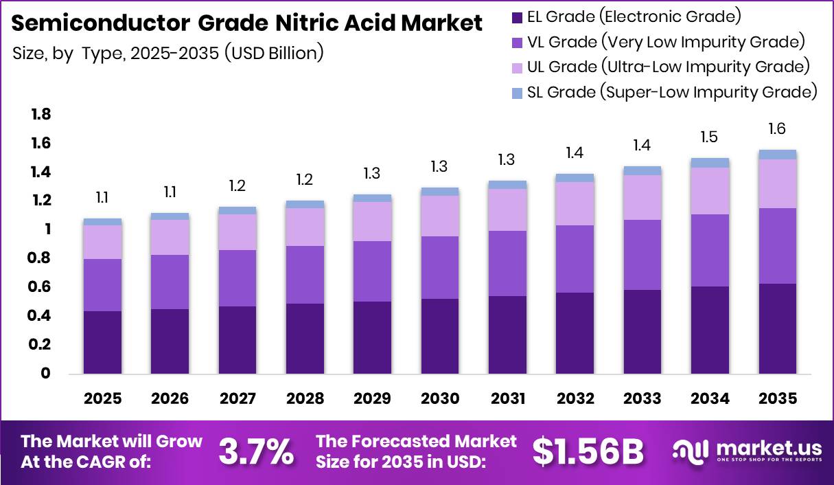
Global Semiconductor Grade Nitric Acid Market size is expected to be worth around USD 1.56 Billion by 2035 from USD 1.1 Billion in 2025, growing at a CAGR of 3.7% during the forecast period 2026 to 2035. This trajectory reflects a market anchored in the structural expansion of semiconductor fabrication capacity worldwide. Producers and investors can expect consistent demand growth tied directly to wafer production volumes.
The semiconductor grade nitric acid market supplies ultra-high-purity HNO₃ used in wet cleaning, oxide etching, and surface treatment steps within integrated circuit and advanced chip manufacturing. This market is segmented by purity grade, including EL, VL, UL, and SL grades, and by application across semiconductor devices, LCD panels, solar energy, and other industrial end uses. The supply chain spans chemical manufacturers, specialty purification facilities, and direct distribution networks serving semiconductor fabrication plants globally.
Key Takeaways
- The global Semiconductor Grade Nitric Acid Market was valued at USD 1.1 Billion in 2025.
- The market is forecast to reach USD 1.56 Billion by 2035, at a CAGR of 3.7% from 2026 to 2035.
- By Type, EL Grade (Electronic Grade) dominates with a 40.5% share in 2025.
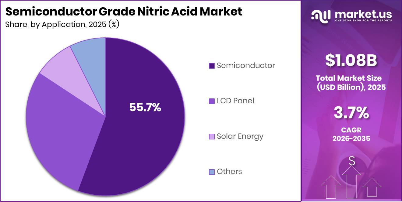
- By Application, Semiconductor holds the leading position with a 55.7% share in 2025.
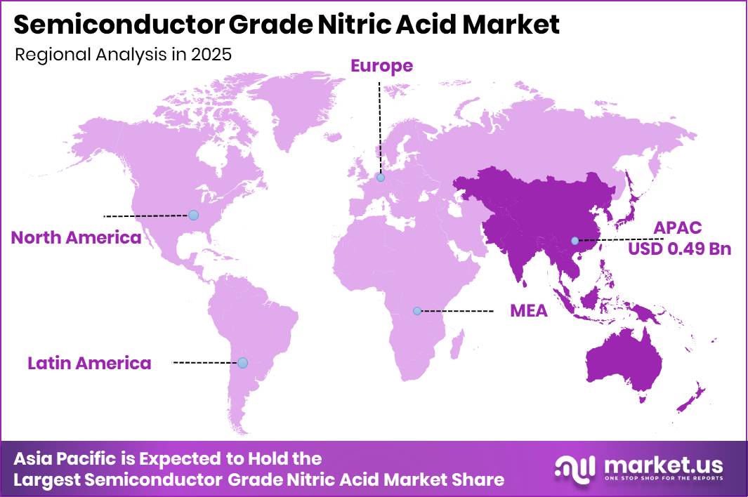
- Asia Pacific is the dominant region with a 45.6% share, valued at USD 0.49 Billion in 2025.
Government-backed semiconductor localization programs across the United States, European Union, Japan, and South Korea are directly shaping demand for qualified local chemical suppliers. These policy frameworks create procurement preferences for regionally produced ultra-pure chemicals. Suppliers that achieve early qualification inside subsidized fab corridors will capture multi-year recurring volumes ahead of later entrants.
According to SEMI, global 300mm semiconductor fab capacity is projected to reach 9.2 million wafers per month in 2025, representing nearly 10% CAGR growth from 2022 levels. This expansion translates directly into higher recurring consumption of semiconductor-grade wet chemicals per operating line. Producers who align capacity additions with fab commissioning timelines will secure the most defensible demand pipelines. As per our research, UBE Corporation announced approximately 30% expansion of its semiconductor-grade high-purity nitric acid production capacity, signaling that leading suppliers are already moving to capture this demand window.
Entegris began initial commercial operations at its Colorado Springs semiconductor manufacturing facility in 2025, bringing advanced filtration and purification technologies closer to major U.S. fabs. This move strengthens domestic materials supply resilience as reshoring policies tighten supplier qualification criteria. This signals a broader industry shift toward localized, contamination-controlled production networks serving next-generation chip architectures.
Type Analysis
EL Grade (Electronic Grade) dominates with 40.5% due to broad baseline compatibility across fab processes.
In 2025, EL Grade (Electronic Grade) held a dominant market position in the By Type segment of the Semiconductor Grade Nitric Acid Market, with a 40.5% share. EL Grade serves as the standard purity tier for a wide range of front-end wet-processing steps, including surface passivation and photoresist strip. This broad applicability across legacy and mid-node fabs makes it the default procurement choice, giving suppliers with certified EL-grade capacity a stable, high-volume base load.
VL Grade (Very Low Impurity Grade) addresses fabs operating at tighter contamination budgets than standard electronic grade permits. Demand for VL Grade tracks closely with capacity additions at sub-28nm nodes, where metallic trace contamination directly affects device yield. Suppliers serving this tier benefit from higher unit margins and longer qualification cycles that raise switching costs for existing customers.
UL Grade (Ultra-Low Impurity Grade) targets the most contamination-sensitive process steps in advanced logic and memory production. As per our research, SEMI C7 Grade 5 ultra-high-purity nitric acid restricts total metallic contamination to less than 100 parts per trillion, illustrating the precision specifications buyers require at this tier. Fabs operating at sub-5nm nodes represent the core buyer segment, and their volume, while smaller, commands significant price premiums that improve supplier margin profiles.
SL Grade (Super-Low Impurity Grade), along with any remaining specialty sub-grades, holds the balance of the market. These tiers serve next-generation applications where purity specifications exceed current industry standards. Early investment in SL Grade qualification positions suppliers to serve leading-edge fabs before these volumes scale into mainstream procurement cycles.
Application Analysis
Semiconductor dominates with 55.7% due to high chemical intensity across front-end wafer processing steps.
In 2025, Semiconductor held a dominant market position in the By Application segment of the Semiconductor Grade Nitric Acid Market, with a 55.7% share. Front-end fab processes including wet etching, oxide growth, and surface cleaning consume ultra-high-purity nitric acid at every wafer pass, creating a recurring per-wafer chemical demand that scales directly with fab utilization. This structural tie to wafer output volumes makes the semiconductor application segment the most predictable revenue base for acid producers.
LCD Panel manufacturing uses nitric acid in thin-film transistor array patterning and substrate cleaning steps. This application segment benefits from continued display capacity investment in Asia, particularly in China and South Korea. However, the shift toward OLED and higher-resolution display technologies introduces process changes that can alter chemical consumption ratios, creating both substitution risk and premium-grade upgrade opportunities for qualified suppliers.
Solar Energy manufacturing uses nitric acid in silicon texturing and passivation processes for photovoltaic cell production. Solar energy capacity additions, particularly in China and Southeast Asia, generate a cost-sensitive demand base that favors lower-purity grades at higher volumes. This creates a distinct commercial tier where acid producers can optimize throughput economics, but margin profiles remain structurally lower than in advanced semiconductor applications.
Others, including specialty chemical synthesis and industrial surface treatment applications, hold the remaining share collectively. These end uses provide volume buffers during semiconductor demand cycles. Producers with flexible purification lines can service this tier without dedicated capacity, improving overall plant utilization between peak fab-qualification campaigns.
Key Market Segments
By Type
- EL Grade (Electronic Grade)
- VL Grade (Very Low Impurity Grade)
- UL Grade (Ultra-Low Impurity Grade)
- SL Grade (Super-Low Impurity Grade)
By Application
- Semiconductor
- LCD Panel
- Solar Energy
- Others
Drivers
Capacity expansion in 300mm fabs entering 2026 to 2027 operations creates a predictable near-term demand ladder for semiconductor-grade wet chemicals. The 2025 SEMI forecast identified 15 new 300mm fab construction starts within the year’s 18 total projects, with most expected to begin operations in 2026 to 2027. Each new operating line generates sequential chemical demand: qualification volumes, pilot-line usage, then full recurring consumption as utilization rises.
According to SEMI, 67 new 300mm fabs and major production-line expansions were scheduled between 2022 and 2025, representing the largest coordinated capacity build-out in the industry’s history. This pipeline compresses the timeline between fab announcement and chemical procurement. Suppliers with pre-positioned qualified inventory near new fab sites will capture first-mover volumes before competitors complete their own qualification processes.
As reported by SEMI, total installed 300mm fab capacity is forecast to grow by 16% in 2025. This single-year capacity jump translates directly into a proportional step-up in ultra-pure chemical consumption across wet-processing lines. Producers that have secured multi-site supply agreements and certified their products across multiple fab qualifications will be insulated from spot-market volatility as this new capacity begins recurring chemical draws.
| Driver | (~) % Impact on CAGR Forecast | Geographic Relevance | Impact Timeline |
|---|---|---|---|
| Advanced-node fab ramp and new cleanroom starts | +1.9% | APAC core, North America core, selective EU | Short term |
| AI server and HPC chip demand lifting wafer intensity | +1.4% | Taiwan, South Korea, U.S., China spill-over | Short term |
| Policy-backed semiconductor localization and chemical sourcing | +1.2% | U.S., EU, Japan, South Korea, India emerging | Medium term |
| Sub-5 nm purity tightening in wet cleaning and etch flows | +1.7% | Taiwan, South Korea, Japan, U.S. advanced-node hubs | Medium term |
| Capacity expansion in 300 mm fabs entering 2026–2027 operations | +1.5% | APAC corridors, North America, Middle East/SE Asia edge nodes | Medium term |
| Supply resilience, on-site blending, and qualification diversification | +0.9% | U.S., Japan, EU, Taiwan | Long term |
Restraints
Environmental compliance costs are tightening margins across the semiconductor wet-chemical supply chain, even where nitric acid itself is not the primary molecule under regulatory review. The EU PFAS restriction proposal advanced materially through 2025 and 2026, with key RAC opinions adopted in 2026 and the process moving toward SEAC and Commission stages. The EU Drinking Water Directive required member-state compliance with PFAS parametric values by January 12, 2026, adding a parallel compliance deadline for chemical facility operators.
In the United States, EPA’s PFAS reporting rule imposed a data-collection burden stretching back to 2011, with deadlines extended into late 2026 and 2027. EHS audits lengthen, wastewater polishing systems require added capital, and customer declarations become more onerous as a result. Compliance programs can absorb 1% to 3% of plant operating cost or USD 1 million to 5 million of site-level annual overhead, lowering returns on expansion projects and slowing multi-site approvals.
Figures from a peer-reviewed environmental study show semiconductor manufacturing facilities recorded a hydrochloric acid emission factor of 0.0017 kg per liter of chemical usage after pollution-control treatment, alongside an ammonia emission factor averaging 0.002 kg per liter of chemical usage. These figures confirm that wet-chemical operations generate measurable regulated emissions even with treatment systems in place. Regulators are using this type of facility-level data to tighten discharge permits, raising the compliance cost baseline for all ultra-pure acid producers and their fab customers.
| Restraint | (~) % Impact on CAGR Forecast | Geographic Relevance | Impact Timeline |
|---|---|---|---|
| Ammonia-cost volatility | -1.4% | EU core, North America, NE Asia | Short term (≤ 2 years) |
| Acid supply tightness | -1.1% | EU, North America, APAC corridors | Short term (≤ 2 years) |
| PFAS/wastewater compliance | -1.0% | EU, U.S., advanced APAC fabs | Medium term (2-4 years) |
| Qualification lock-in | -0.9% | Global Tier-1 fab clusters | Medium term (2-4 years) |
| China-linked trade friction | -0.8% | U.S.-China lanes, Korea, Taiwan, Japan | Medium term (2-4 years) |
| Utility and purity inflation | -0.7% | EU core, Japan, Korea, U.S. | Long term (≥ 4 years) |
Challenges
Demand for ultra-pure wet chemicals is moving into newly subsidized semiconductor corridors faster than localized specialty acid ecosystems can be replicated. A timing gap has opened between fab ramp announcements and nearby qualified chemical supply, particularly in Europe and the United States where chemical localization is newer than in Taiwan, South Korea, and Japan. This mismatch creates an estimated 1.2 percentage-point CAGR friction drag as order books remain healthy but conversion into stable local recurring volume is delayed.
In April 2025, BASF announced a high double-digit million-euro investment to build a new semiconductor-grade sulfuric acid production facility at Ludwigshafen, Germany. This facility is only expected to start operations in 2027, illustrating that even adjacent ultra-pure acid investments require multi-year synchronization with customer capacity additions. By analogy, nitric acid suppliers face 18 to 36-month windows where regional demand is real but fulfillment still depends on longer-haul imports, qualification duplication, and higher safety stock.
The operational response to this mismatch is forcing suppliers to adopt hub-and-spoke tank storage, multi-region toll purification strategies, and staggered contracting that prioritizes anchor fabs over broad merchant expansion. These adaptations raise logistics and overhead costs per unit sold. Suppliers that invest in regional purification and packaging infrastructure now will close the qualification gap before competitors, converting the current friction into a structural supply moat.
| Challenge | (~) % CAGR Friction Drag | Geographic Relevance | Mitigation Horizon |
|---|---|---|---|
| Purity Yield Volatility | -1.4% | APAC fab clusters, North America new fabs, EU specialty chemical hubs | Medium term (2-4 years) |
| Regional Capacity Mismatch | -1.2% | Europe emerging hubs, US reshoring corridors, Taiwan-Korea incumbents | Medium term (2-4 years) |
| Energy And Utility Intensity | -0.9% | EU regulatory hubs, US Southwest fabs, water-stressed Asian corridors | Long term (≥ 4 years) |
| Skilled Labor Bottlenecks | -1.1% | US greenfield fabs, EU expansion zones, advanced APAC nodes | Long term (≥ 4 years) |
| Hazardous Logistics Fragility | -0.8% | Cross-border APAC lanes, transatlantic supply routes, inland fab networks | Short term (≤ 2 years) |
| Compliance And Traceability Load | -0.7% | EU regulatory hubs, North America qualification chains, Japan-Korea quality systems | Medium term (2-4 years) |
Opportunities
The EU PFAS restriction proposal is moving toward sector-specific controls, with semiconductor uses likely permitted only under conditional derogations, strict emission controls, and lifecycle reporting. Individual PFAS thresholds of 25 ppb and total PFAS thresholds of 250 ppb are already framing compliance design choices for fab operators. Suppliers that engineer validated mixed-chemistry systems around nitric acid can reduce customers’ regulatory burden and shorten audit cycles by an estimated 10 to 20 percent.
Nitric acid is not a universal substitute for fluorinated chemistries, but in selected cleaning and oxide-treatment workflows, reformulated processes can command 5 to 10 percent compliance premia. If even a modest share of wet benches in Europe, Japan, and North America transitions toward lower-fluorine process windows over 2028 to 2032, the resulting adjacent total addressable market expansion supports approximately 1.2 percentage points of CAGR upside beyond the market’s existing trajectory. This converts a compliance burden into a product differentiation lever for technically advanced suppliers.
Acid reclaim and closed-loop service models represent a structurally distinct growth avenue, particularly in water-stressed APAC corridors and the U.S. Southwest where discharge regulations are tightening independently of PFAS rules. A 2025 semiconductor wastewater recycling project demonstrated recovery of nitric acid using sub-atmospheric thermoseparation, enabling selective reclamation of HNO₃ from manufacturing waste streams in a validated pilot-plant environment. Suppliers that commercialize recovery services capture both a recurring service revenue stream and a differentiated environmental compliance offering.
| Opportunity | (~) % Potential CAGR Upside | Geographic Relevance | Execution Window |
|---|---|---|---|
| Local-for-local fab qualification | +2.0% | North America core, EU, Japan | Short term |
| Advanced packaging chemical bundles | +1.7% | Taiwan, South Korea, Singapore, Malaysia | Short term |
| Acid reclaim and closed-loop services | +1.4% | Water-stressed APAC, US Southwest | Medium term |
| PFAS-shift cleaning substitution | +1.2% | EU, North America, Japan | Medium term |
| Ultra-premium trace-metal grades | +1.0% | Leading-edge fabs in Taiwan, US, Korea | Short term |
| Regional M&A and toll purification roll-up | +0.8% | India, Southeast Asia, EU | Long term |
Regional Analysis
Asia Pacific Dominates the Semiconductor Grade Nitric Acid Market with a Market Share of 45.6%, Valued at USD 0.49 Billion
Asia Pacific commands 45.6% of the global market, driven by the concentration of the world’s largest semiconductor fabrication clusters in Taiwan, South Korea, Japan, and China. These countries host the majority of advanced-node and high-volume fabs that require continuous ultra-pure chemical supply. In December 2025, Merck KGaA confirmed its Kaohsiung Semiconductor Solutions Megasite will begin production in 2026 and add 150 new jobs, reinforcing Taiwan’s position as a critical regional supply anchor.
North America holds a structurally growing position as U.S. semiconductor reshoring policy drives new fab starts in Arizona, Texas, and Ohio. Federal incentives under domestic chip legislation are accelerating fab qualification timelines and creating immediate demand for locally sourced ultra-pure process chemicals. Suppliers that establish certified U.S. production ahead of fab ramp schedules will be positioned to capture long-term supply agreements at premium domestic pricing.
Europe is building out its semiconductor materials infrastructure, though supply localization lags regional fab ambitions. The EU Chips Act is directing investment toward new fabrication facilities in Germany, the Netherlands, and Ireland. In September 2025, Fujifilm Electronic Materials announced evaluation of a semiconductor materials facility in India, reflecting broader industry interest in emerging Asian corridors beyond the established APAC core and pointing toward supply diversification strategies across the wider region.
Key Regions and Countries
North America
- US
- Canada
Europe
- Germany
- France
- The UK
- Spain
- Italy
- Rest of Europe
Asia Pacific
- China
- Japan
- South Korea
- India
- Australia
- Rest of APAC
Latin America
- Brazil
- Mexico
- Rest of Latin America
Middle East and Africa
- GCC
- South Africa
- Rest of MEA
Key Company Insights
Honeywell International Inc. holds a strategic position in the semiconductor-grade chemicals market through its integrated specialty chemicals and advanced materials divisions. Its global manufacturing footprint and established fab qualification credentials create high switching costs for existing customers. However, its diversified conglomerate structure means semiconductor chemicals must compete internally for capital allocation against larger industrial segments.
BASF is actively expanding its electronic chemicals manufacturing footprint in Europe, positioning itself as a preferred local supplier to emerging EU semiconductor fabs. In January 2025, Fujifilm announced a plan to invest approximately ¥100 billion, about US$640 million, by March 2027 to expand semiconductor materials production across Japan, the United States, South Korea, and other strategic regions, intensifying competition for the same advanced-node customer base that BASF is targeting in Europe.
Key Players
- Honeywell International Inc.
- BASF
- The Chemours Company
- DuPont
- Yara International
- Sumitomo Chemical Co., Ltd.
- Vizag Chemicals
- Columbus Chemicals
- Lab Alley
- Ing. Petr Švec – PENTA s.r.o.
- PerkinElmer
- Alliance Chemical
- ECOLINK
- Other Key Players
Recent Developments
- October 2025 – BASF announced construction of a new Electronic Grade Ammonium Hydroxide (NH₄OH EG) plant in Ludwigshafen, Germany, to supply ultra-pure chemicals for wafer cleaning and etching processes in advanced semiconductor manufacturing.
- December 2025 – Merck KGaA inaugurated its €500 million Semiconductor Solutions Megasite in Kaohsiung, Taiwan, creating its largest semiconductor materials campus worldwide to manufacture thin films, specialty gases, and formulation materials for next-generation AI and memory chips.
- December 2025 – Merck KGaA reported that its Electronics business had invested more than €3 billion globally since 2021 under its “Level Up” program, expanding semiconductor materials production capacity and technology capabilities near major chip manufacturing customers.
- February 2025 – Fujifilm announced a ¥4 billion investment in its Belgium facility to add new production lines for CMP slurries and advanced photolithography-related semiconductor materials, supporting semiconductor demand growth in Europe.
- August 2025 – Entegris announced a US$700 million investment program in the United States to expand semiconductor materials R&D and establish a new Technology Center in Aurora, Illinois, focused on deposition materials, cleans, slurries, and CMP technologies.
- November 2025 – Entegris officially opened its 135,000-square-foot Colorado Springs Manufacturing Center of Excellence, expanding domestic production of advanced purification and contamination-control solutions used throughout semiconductor chemical supply chains.
- 2025 – DSM Semichem secured a US$7.87 million grant from the Texas Semiconductor Innovation Fund to support expansion of its electronic-grade sulfuric acid production facility in Plainview, Texas, a project involving total capital investment of US$176 million.
- 2025 – MKS Instruments initiated the divestiture of a non-core specialty chemicals business valued at approximately US$1 billion, allowing the company to focus on semiconductor manufacturing technologies and materials serving advanced chip production.
Report Scope
| Report Features | Description |
|---|---|
| Market Value (2025) | USD 1.1 Billion |
| Forecast Revenue (2035) | USD 1.56 Billion |
| CAGR (2026-2035) | 3.7% |
| Base Year for Estimation | 2025 |
| Historic Period | 2020-2024 |
| Forecast Period | 2026-2035 |
| Report Coverage | Revenue Forecast, Market Dynamics, Market Opportunity Analysis, Technology and Innovation Landscape, Competitive Landscape, Recent Developments |
| Segments Covered | By Type (EL Grade, VL Grade, UL Grade, SL Grade); By Application (Semiconductor, LCD Panel, Solar Energy, Others) |
| Regional Analysis | North America (US and Canada), Europe (Germany, France, The UK, Spain, Italy, and Rest of Europe), Asia Pacific (China, Japan, South Korea, India, Australia, and Rest of APAC), Latin America (Brazil, Mexico, and Rest of Latin America), Middle East and Africa (GCC, South Africa, and Rest of MEA) |
| Competitive Landscape | Honeywell International Inc., BASF, The Chemours Company, DuPont, Yara International, Sumitomo Chemical Co., Ltd., Vizag Chemicals, Columbus Chemicals, Lab Alley, Ing. Petr Švec – PENTA s.r.o., PerkinElmer, Alliance Chemical, ECOLINK, Other Key Players |
| Customization Scope | Customization for segments, region/country-level will be provided. Additional customization can be done based on requirements. |
| Purchase Options | We have three licenses to opt for: Single User License, Multi-User License (Up to 5 Users), Corporate Use License (Unlimited User and Printable PDF) |