Global Semiconductor Wafer Inspection Equipment Market Size, Share, Statistics Analysis Report By Type (Optical Wafer Inspection Equipment, E-Beam Wafer Inspection Equipment, Other Types), By Application (Wafer Inspection, Package Inspection, Chip Inspection), By End-User (Semiconductor Manufacturers, Foundries, Integrated Device Manufacturers (IDMs), OSAT (Outsourced Semiconductor Assembly and Test)), Region and Companies - Industry Segment Outlook, Market Assessment, Competition Scenario, Trends and Forecast 2025-2034
- Published date: Feb 2025
- Report ID: 141438
- Number of Pages: 372
- Format:
-
keyboard_arrow_up
Quick Navigation
Report Scope
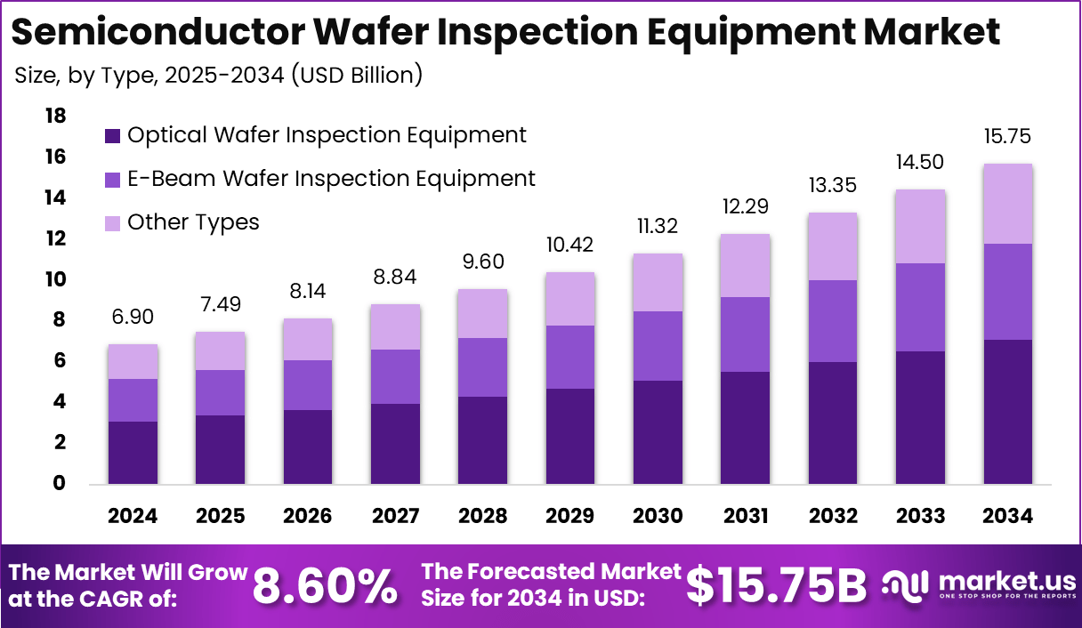
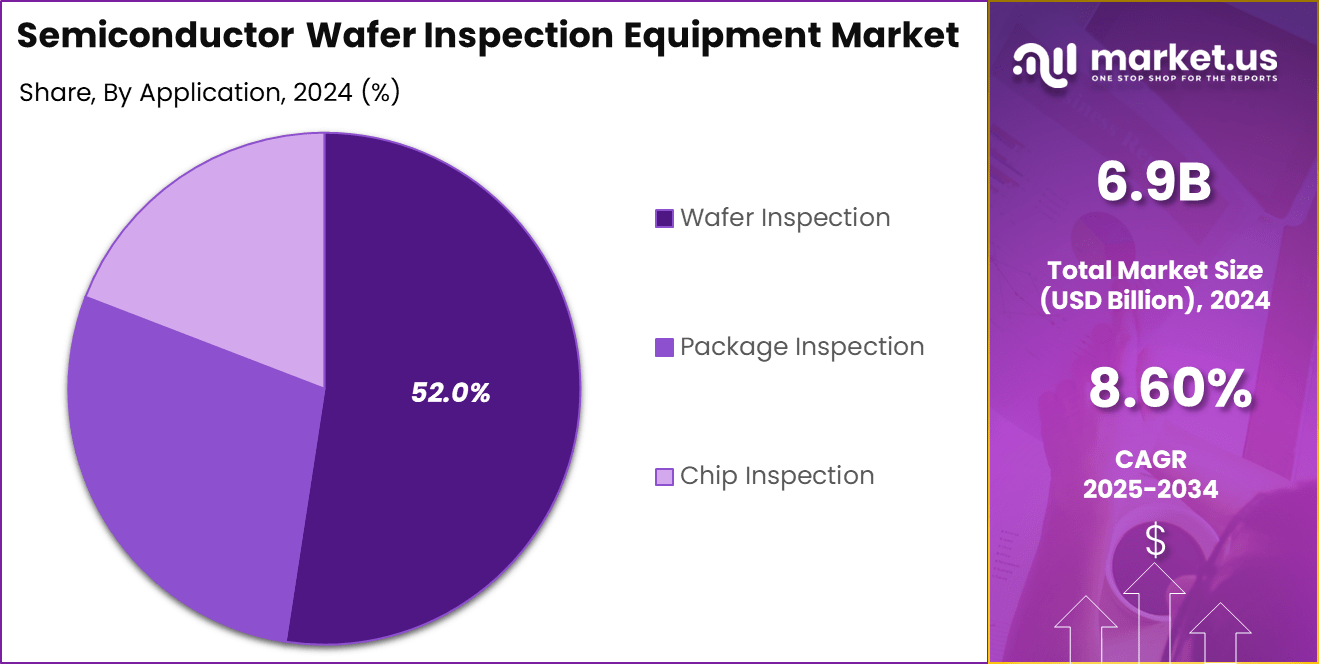
The Global Semiconductor Wafer Inspection Equipment Market is expected to be worth around USD 15.75 Billion by 2034, up from USD 6.9 Billion in 2024. It is expected to grow at a CAGR of 8.60% from 2025 to 2034.
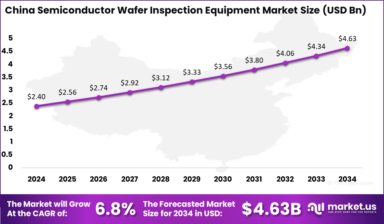
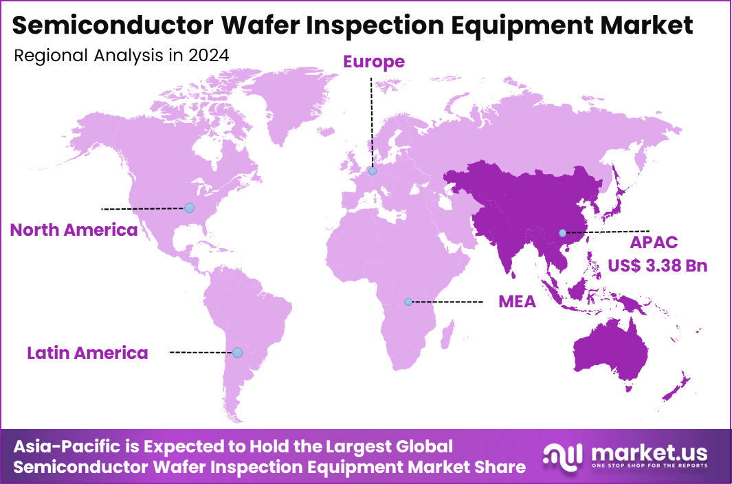
In 2024, Asia-Pacific held a dominant market position, capturing over a 49% share and earning USD 3.38 Billion in revenue. Further, China dominates the market by USD 2.4 Billion, steadily holding a strong position with a CAGR of 6.8%.
The Semiconductor Wafer Inspection Equipment market is a critical segment within the semiconductor industry, focusing on advanced systems used to inspect and analyze semiconductor wafers during manufacturing. These systems ensure the quality and precision required to meet the ever-increasing demand for smaller, faster, and more powerful electronic devices.
As semiconductor manufacturing processes become more intricate, the role of wafer inspection equipment in detecting defects and ensuring yield quality becomes even more important. The market for these inspection tools is projected to grow significantly, driven by factors like increased demand for advanced electronics, automation in production, and rising complexity in semiconductor designs.
Several key factors are propelling the growth of the Semiconductor Wafer Inspection Equipment market. The primary driver is the increasing demand for smaller and more efficient semiconductor devices, which requires highly precise inspection during production. As consumer electronics, especially smartphones, AI chips, and 5G infrastructure, continue to evolve, manufacturers require cutting-edge inspection equipment to ensure the quality and reliability of wafers.
Furthermore, the rise of Internet of Things (IoT) and autonomous vehicles is boosting the need for high-performance semiconductors, driving the demand for advanced inspection technologies. Another factor contributing to the market’s growth is the ongoing push for miniaturization and the development of 3D semiconductor packaging, both of which require more advanced inspection systems to detect micro-level defects and ensure functional integrity.
Key Takeaways
- 2024 Market Value: The Semiconductor Wafer Inspection Equipment market is valued at USD 6.9 billion in 2024.
- Projected Market Value: The market is projected to grow significantly, reaching USD 15.75 billion by 2034.
- CAGR: The market is expected to grow at a robust CAGR of 8.60% from 2024 to 2034.
- By Type: The Optical Wafer Inspection Equipment segment holds the largest share, capturing 45% of the market.
- By Application: Wafer Inspection is the dominant application, accounting for 52% of the market.
- By End-User: Semiconductor Manufacturers are the largest end-users, with a market share of 40%.
- Regional Breakdown: Asia-Pacific dominates the market with a share of 49%, driven by major semiconductor production hubs.
- China’s Market: China holds a significant portion of the market with a value of USD 2.4 billion and a CAGR of 6.8%.
Analyst Review
The demand for Semiconductor Wafer Inspection Equipment is surging due to the increasing complexity in the semiconductor manufacturing process. As semiconductor fabs move to advanced nodes such as 5nm and 3nm for more powerful and efficient chips, the need for precise inspection technologies grows.
The demand is particularly high in regions like Asia-Pacific, which houses the largest semiconductor production hubs, including Taiwan, South Korea, and China. These regions are investing heavily in cutting-edge inspection technologies to maintain their global leadership in semiconductor manufacturing.
One of the significant opportunities in the Semiconductor Wafer Inspection Equipment market lies in the growing adoption of AI-driven inspection systems. These systems use machine learning algorithms to improve defect detection and classification, thus reducing human error and increasing inspection speed. As chip manufacturers move towards smarter automation and Industry 4.0 principles, integrating AI and big data analytics into wafer inspection becomes more feasible and beneficial.
Another opportunity lies in the increasing demand for next-generation semiconductor technologies such as quantum computing and silicon photonics. These technologies require highly specialized inspection tools to ensure they meet the stringent performance requirements. With emerging applications in 5G, automotive electronics, and healthcare devices, the need for advanced wafer inspection equipment is expected to expand across multiple sectors.
Technological advancements in the Semiconductor Wafer Inspection Equipment market are largely centered around the integration of AI, machine learning, and high-resolution imaging technologies. Modern inspection systems utilize optical inspection and electron microscopy to detect surface defects at the microscopic and even atomic levels. The introduction of deep learning algorithms has revolutionized defect classification by enabling equipment to identify and predict defect patterns more accurately than traditional methods.
Additionally, non-destructive testing (NDT) methods, such as X-ray inspection and atomic force microscopy, are gaining traction due to their ability to inspect the internal structure of wafers without causing damage. The adoption of advanced 3D imaging techniques is also enabling more accurate defect detection in complex 3D semiconductor packages. These technological innovations are reducing inspection times, increasing throughput, and ensuring the highest quality in semiconductor manufacturing, thus pushing the market towards higher precision and efficiency.
Key Statistics
Quantity
- Units Sold (2023): Estimated at around 1,500 to 2,000 units globally.
- Installed Base (2023): Approximately 10,000 to 12,000 units worldwide.
End-Users
- Foundries: Generate around 45% of the revenue in 2024.
- IDMs (Integrated Device Manufacturers): Contribute approximately 30% of the revenue.
Applications
- Defect Detection: Used in about 80% of inspection processes.
- Metrology/Measurement: Accounts for around 15% of applications.
- Overlay Inspection: Used in about 5% of applications.
Regional Presence
- Asia-Pacific: Accounts for about 55% of the global market.
- North America: Represents around 25% of the market.
- Europe: Contributes approximately 15% of the market.
Technological Trends
- Advancements in AI and Machine Learning: Expected to enhance inspection accuracy by up to 20% by 2026.
- High-Speed Inspection Capabilities: Can inspect up to 100 wafers per hour with advanced systems.
Regional Analysis
China Region Market Size
In Asia-Pacific, China dominates the semiconductor wafer inspection equipment market with a market size of USD 2.4 billion. This position is reinforced by China’s robust semiconductor manufacturing ecosystem, which continues to expand rapidly.
The country’s large-scale investments in semiconductor production, along with government initiatives to promote self-sufficiency in chip manufacturing, contribute significantly to its strong foothold in the market. As China’s semiconductor industry evolves, there is an increasing demand for precision and efficiency in the manufacturing process, making wafer inspection equipment indispensable.
In addition to its market size, China is expected to continue growing at a CAGR of 6.8%, driven by the need for advanced technologies to meet the rising demand for next-generation chips. As Chinese semiconductor manufacturers focus on developing cutting-edge semiconductors for applications in 5G, AI, and IoT, they are increasingly adopting sophisticated wafer inspection systems to ensure high quality and yield in their production lines.
The dominance of China within the Asia-Pacific region is further supported by its extensive semiconductor supply chain, which includes both foundries and fabless companies. This allows the country to continue leading not only in wafer inspection equipment but also in the overall semiconductor manufacturing process, helping it maintain a strategic edge in the global market.
Asia Pacific Market Size
In 2024, Asia-Pacific held a dominant market position in the Semiconductor Wafer Inspection Equipment market, capturing more than 49% of the global share, equivalent to USD 3.38 billion in revenue. This region’s strong position is largely driven by the presence of major semiconductor manufacturing hubs, particularly in countries like Taiwan, South Korea, Japan, and China.
These countries are at the forefront of semiconductor production, and as the demand for advanced chips grows across industries such as telecommunications, consumer electronics, and automotive, the need for high-precision wafer inspection systems becomes even more critical.
Asia-Pacific’s dominance is further reinforced by its substantial investment in semiconductor fabrication plants (fabs) and the increasing complexity of semiconductor designs. As manufacturing processes move to smaller nodes, such as 7nm and 5nm, inspection equipment plays a crucial role in ensuring wafer quality and yield.
This need is heightened by the expanding focus on advanced technologies, including 5G infrastructure, AI chips, and IoT devices, which all require flawless semiconductor components. The region’s significant share also reflects the ongoing trend of global manufacturers relocating their production to Asia-Pacific, where the cost-effectiveness of semiconductor production is coupled with technological advancements.
The market in China, in particular, has been a key driver within the region, with a growing emphasis on domestic production and reduced reliance on external suppliers. With a market value of USD 2.4 billion and a steady CAGR of 6.8%, China is set to maintain its leadership role in wafer inspection equipment, supported by strong government initiatives and a thriving semiconductor ecosystem.
As the region continues to advance, Asia-Pacific will remain a critical hub for the development and deployment of cutting-edge semiconductor inspection technologies, ensuring it retains its dominant market share in the coming years.
By Type
In 2024, the Optical Wafer Inspection Equipment segment held a dominant market position, capturing more than 45% of the global market share. This leadership can be attributed to the widespread adoption of optical inspection systems in semiconductor manufacturing, which are essential for detecting defects on the wafer’s surface.
Optical inspection systems use light-based technologies, such as laser scanning and high-resolution imaging, to identify surface imperfections at a microscopic level. The popularity of optical systems is driven by their ability to provide fast, non-destructive inspection with high throughput, which is crucial in high-volume manufacturing environments.
Moreover, the advancements in resolution and speed of optical inspection systems have made them more efficient and accurate, which is critical as semiconductor devices continue to shrink in size and increase in complexity. As the demand for smaller, more powerful chips grows with applications in areas such as 5G, AI, and IoT, the need for precise wafer inspection increases. The versatility of optical inspection systems in handling a wide range of wafer sizes and materials further solidifies their leading position in the market, ensuring their continued dominance over other types of inspection technologies.
By Application
In 2024, the Wafer Inspection segment held a dominant market position, capturing more than 52% of the global market share. This dominance is largely due to the critical role wafer inspection plays in the semiconductor manufacturing process. Wafer inspection is essential for detecting defects and ensuring the integrity of semiconductor wafers before they undergo further processing.
As semiconductor manufacturing advances to smaller nodes, such as 7nm and 5nm, the need for high-precision inspection systems becomes even more vital. The wafer is the foundation of the chip, and any defects at this stage can impact the entire production cycle, leading to reduced yields and higher costs.
The growing demand for high-performance chips used in 5G, AI, and IoT applications further drives the demand for wafer inspection. As these technologies require ever-smaller and more intricate designs, the importance of early defect detection and precise measurements is paramount.
The ability to inspect wafers at high resolution and with minimal damage makes wafer inspection systems indispensable. This, coupled with the increasing complexity of semiconductor devices, ensures that wafer inspection continues to be the leading application in the semiconductor wafer inspection equipment market.
By End-User
In 2024, the Semiconductor Manufacturers segment held a dominant market position, capturing more than 40% of the global market share. This dominance is driven by the crucial role semiconductor manufacturers play in the overall semiconductor supply chain.
These manufacturers are responsible for the fabrication of wafers, where precision and defect-free products are essential to achieving high yields and ensuring the quality of final semiconductor devices. As semiconductor technology continues to advance, particularly with the shift to smaller process nodes like 5nm and 3nm, the demand for sophisticated inspection equipment has escalated. Manufacturers must detect minute defects early in the production process to prevent costly errors later on.
Furthermore, the growing demand for advanced semiconductors in emerging applications like 5G, AI, autonomous vehicles, and IoT requires strict quality control, adding to the need for high-precision inspection systems.
Semiconductor manufacturers must invest in state-of-the-art wafer inspection equipment to remain competitive and maintain product reliability. The industry’s focus on increasing automation, reducing production costs, and improving yield rates further cements the dominant role of semiconductor manufacturers in driving the growth of the wafer inspection equipment market.
Key Market Segments
By Type
- Optical Wafer Inspection Equipment
- E-Beam Wafer Inspection Equipment
- Other Types
By Application
- Wafer Inspection
- Package Inspection
- Chip Inspection
By End-User
- Semiconductor Manufacturers
- Foundries
- Integrated Device Manufacturers (IDMs)
- OSAT (Outsourced Semiconductor Assembly and Test)
Driving Factors
Rising Demand for Advanced Semiconductor Devices
The rising demand for advanced semiconductor devices is one of the key driving factors for the growth of the Semiconductor Wafer Inspection Equipment market. As technologies like 5G, artificial intelligence (AI), autonomous vehicles, and the Internet of Things (IoT) continue to evolve, the need for high-performance, smaller, and more efficient semiconductor chips is growing exponentially. These applications require chips that are both powerful and reliable, with zero defects in their semiconductor wafers.
In response to this demand, semiconductor manufacturers are turning to advanced wafer inspection systems to maintain quality and increase yield rates. As semiconductor processes shrink and become more complex, the need for high-precision inspection tools becomes crucial to detect even the tiniest defects that could affect performance.
Wafer inspection is becoming more important as chips continue to scale down to sub-5nm nodes, where traditional inspection methods may no longer be effective. The growing shift toward 3D packaging and multi-layered chips also adds complexity, further driving the need for robust wafer inspection technologies to ensure the reliability of these next-gen chips.
Restraining Factors
High Cost of Advanced Wafer Inspection Systems
A major restraining factor for the Semiconductor Wafer Inspection Equipment market is the high cost of advanced inspection systems. Wafer inspection equipment, particularly those based on sophisticated technologies like e-beam inspection or atomic force microscopy, can be prohibitively expensive for smaller semiconductor companies or fabless manufacturers. These high initial costs, along with the ongoing maintenance, calibration, and software upgrades required, can limit accessibility to cutting-edge inspection systems for smaller players in the industry.
The costs associated with these technologies are not just a barrier for smaller businesses but can also hinder the widespread adoption of some of the more advanced inspection methods. Even though these systems can significantly improve yield rates and product quality, the capital-intensive nature of the equipment presents a challenge for companies with limited budgets. As a result, many smaller semiconductor manufacturers and companies in emerging markets may delay or avoid investing in high-end inspection systems, which could slow down overall market growth.
Growth Opportunities
AI and Machine Learning Integration
A promising growth opportunity in the Semiconductor Wafer Inspection Equipment market lies in the integration of AI and machine learning (ML) technologies. The application of AI and ML to wafer inspection equipment allows for more accurate defect detection and predictive analytics, which significantly enhances the overall inspection process. As semiconductor manufacturing processes become more complex, traditional methods of inspection often fall short, leading to higher chances of missed defects or false positives.
AI-powered inspection systems, on the other hand, can automatically identify patterns in the data and learn from them, making defect detection faster and more reliable. These AI-driven systems not only improve the speed of inspections but also increase the throughput of semiconductor fabs, leading to reduced production costs.
As the demand for next-gen semiconductors continues to grow, the role of AI and ML in wafer inspection becomes even more critical. AI can assist in handling massive volumes of data generated by high-resolution inspection tools and provide real-time feedback to manufacturers, enabling them to make quick adjustments to improve yield.
Challenging Factors
Complexity of Advanced Semiconductor Manufacturing
A major challenge facing the Semiconductor Wafer Inspection Equipment market is the increasing complexity of advanced semiconductor manufacturing. As the semiconductor industry moves toward smaller nodes and more advanced architectures, such as 3D packaging and multi-layered chips, the inspection of wafers becomes significantly more challenging. Defects that may have been easily detectable at larger nodes are harder to spot at sub-5nm scales, where even the slightest imperfection can lead to product failure.
The introduction of new materials, such as compound semiconductors and 2D materials, further complicates the wafer inspection process. These new materials often behave differently under inspection, requiring new techniques and technologies to detect defects accurately. The need for high-resolution imaging systems and the capability to inspect multi-layered devices without damaging the structure adds to the overall complexity.
Growth Factors
Increasing Demand for Advanced Chips
The demand for advanced semiconductors continues to drive growth in the Semiconductor Wafer Inspection Equipment market. As technologies like 5G, AI, autonomous vehicles, and IoT require more powerful and smaller chips, the need for high-quality, defect-free semiconductors is paramount. This trend is pushing semiconductor manufacturers to adopt state-of-the-art wafer inspection technologies to ensure the performance and reliability of these next-generation chips.
By 2034, the market is projected to grow to USD 15.75 billion, with a CAGR of 8.6%. As semiconductor manufacturing processes move towards sub-5nm nodes, wafer inspection equipment will play an increasingly crucial role in defect detection and yield optimization. With semiconductor applications expanding globally, especially in Asia-Pacific and the US, the market is set to experience sustained demand for advanced wafer inspection solutions.
Emerging Trends
AI and Automation in Wafer Inspection
One of the most significant emerging trends in the semiconductor wafer inspection industry is the integration of artificial intelligence (AI) and automation. AI is transforming inspection processes by offering improved defect detection capabilities and predictive analytics. In 2024, AI-powered wafer inspection systems are expected to gain more traction, enhancing detection accuracy while reducing human error.
Additionally, automation in semiconductor fabs is helping to streamline operations and boost productivity. These AI and automation advancements are anticipated to grow the market by making inspections faster, more reliable, and cost-efficient, catering to the growing demand for precision and high-throughput manufacturing. Companies that can incorporate AI-driven solutions into their inspection equipment will be better positioned to meet the increasing complexity and scale of semiconductor production.
Business Benefits
Enhanced Yield and Reduced Costs
Investing in advanced wafer inspection equipment provides semiconductor manufacturers with significant business benefits, the most notable being improved yield rates and reduced production costs. The ability to identify defects early in the production process helps manufacturers avoid costly defects later, improving the overall efficiency of the production line.
By adopting cutting-edge technologies such as e-beam inspection and optical inspection systems, manufacturers can ensure that only defect-free wafers move on to the next stages of production, reducing scrap rates. This, in turn, drives cost savings and increases profitability. The integration of AI and machine learning further optimizes the process, enabling real-time data analysis and predictive maintenance.
As a result, manufacturers can reduce downtime, maximize equipment lifespan, and improve overall fab efficiency. The market for wafer inspection equipment is projected to expand significantly as more companies recognize the value these technologies bring in terms of improved quality control and cost reduction.
Key Regions and Countries
- North America
- US
- Canada
- Europe
- Germany
- France
- The UK
- Spain
- Italy
- Russia
- Netherlands
- Rest of Europe
- Asia Pacific
- China
- Japan
- South Korea
- India
- Australia
- Singapore
- Thailand
- Vietnam
- Rest of APAC
- Latin America
- Brazil
- Mexico
- Rest of Latin America
- Middle East & Africa
- South Africa
- Saudi Arabia
- UAE
- Rest of MEA
Key Player Analysis
Honeywell International Inc. is a prominent player in the semiconductor wafer inspection equipment market, known for its technological innovations and broad industrial footprint. The company has been actively expanding its presence in this sector through acquisitions and strategic partnerships. For instance, in recent years, Honeywell has invested heavily in automation and AI-based inspection systems, enhancing its capabilities in wafer inspection.
Bosch Security Systems is another key player in the semiconductor wafer inspection equipment market. The company has been focused on developing cutting-edge optical inspection solutions for semiconductor manufacturers. Bosch’s entry into the semiconductor sector comes with a strong legacy of precision engineering and sensor technologies. The company is known for its innovative sensor-based inspection systems that offer enhanced defect detection, essential for the shrinking process nodes in the semiconductor industry.
Hikvision Digital Technology Co., Ltd., primarily recognized for its expertise in video surveillance systems, has also become a key player in the semiconductor wafer inspection equipment space. The company has leveraged its core competencies in machine vision technology to develop advanced inspection solutions for the semiconductor industry. In recent years, Hikvision has made significant strides in integrating AI and big data analytics into its inspection systems, providing real-time, high-precision defect detection for semiconductor wafers.
Top Key Players in the Market
- Applied Materials Inc.
- ASML Holding NV
- Microtronic
- Toray Industries Inc.
- Tokyo Electron Limited
- KLA-Tencor
- Hitachi High-TecCorp.
- Nikon Corp.
- SCREEN Holdings Co. Ltd.
- Advantest Corporation
- Bruker Corp.
- Teradyne Inc.
- Lasertec Corp.
- Cognex Corp.
- JEOL Ltd.
- Onto Innovation Inc.
- Veeco Instruments Inc.
- Cohu Inc.Nova Measuring Instruments Ltd.
- SUSS MicroTec Inc.
- Camtek Ltd.
- Nanometrics Inc.
- Ueno Seiki
- Rudolph Technology & Associates
- Carl Zeiss AG
- Other Key Players
Recent Developments
- In 2024, Honeywell International launched a new AI-powered wafer inspection system, integrating advanced machine learning algorithms to enhance defect detection at sub-5nm nodes.
- In 2024, Hikvision introduced a cutting-edge optical inspection tool with integrated real-time analytics, aimed at increasing wafer yield and optimizing semiconductor production lines.
Report Scope
Report Features Description Market Value (2024) USD 6.9 Billion Forecast Revenue (2034) USD 15.75 Billion CAGR (2025-2034) 8.60% Largest Market North America Base Year for Estimation 2024 Historic Period 2020-2023 Forecast Period 2025-2034 Report Coverage Revenue Forecast, Market Dynamics, Competitive Landscape, Recent Developments Segments Covered By Type (Optical Wafer Inspection Equipment, E-Beam Wafer Inspection Equipment, Other Types), By Application (Wafer Inspection, Package Inspection, Chip Inspection), By End-User (Semiconductor Manufacturers, Foundries, Integrated Device Manufacturers (IDMs), OSAT (Outsourced Semiconductor Assembly and Test)) Regional Analysis North America (US, Canada), Europe (Germany, UK, Spain, Austria, Rest of Europe), Asia-Pacific (China, Japan, South Korea, India, Australia, Thailand, Rest of Asia-Pacific), Latin America (Brazil), Middle East & Africa(South Africa, Saudi Arabia, United Arab Emirates) Competitive Landscape Honeywell International Inc., Bosch Security Systems, Hikvision Digital Technology Co., Ltd., SimpliSafe, Inc., Ring LLC (Amazon), Nest Labs (Google), Samsung Electronics Co., Ltd., Panasonic Corporation, Sony Corporation, FLIR Systems, Inc., Johnson Controls International plc, Schneider Electric SE, ABB Ltd., Securitas AB, Assa Abloy AB, Other Key Players Customization Scope We will provide customization for segments and at the region/country level. Moreover, additional customization can be done based on the requirements. Purchase Options We have three licenses to opt for Single User License, Multi-User License (Up to 5 Users), Corporate Use License (Unlimited User and Printable PDF)  Semiconductor Wafer Inspection Equipment MarketPublished date: Feb 2025add_shopping_cartBuy Now get_appDownload Sample
 -
-
- Applied Materials Inc.
- ASML Holding NV
- Microtronic
- Toray Industries Inc.
- Tokyo Electron Limited
- KLA-Tencor
- Hitachi High-TecCorp.
- Nikon Corp.
- SCREEN Holdings Co. Ltd.
- Advantest Corporation
- Bruker Corp.
- Teradyne Inc.
- Lasertec Corp.
- Cognex Corp.
- JEOL Ltd.
- Onto Innovation Inc.
- Veeco Instruments Inc.
- Cohu Inc.Nova Measuring Instruments Ltd.
- SUSS MicroTec Inc.
- Camtek Ltd.
- Nanometrics Inc.
- Ueno Seiki
- Rudolph Technology & Associates
- Carl Zeiss AG
- Other Key Players
Our Clients
- 141438
- Feb 2025