Quick Navigation
Report Overview
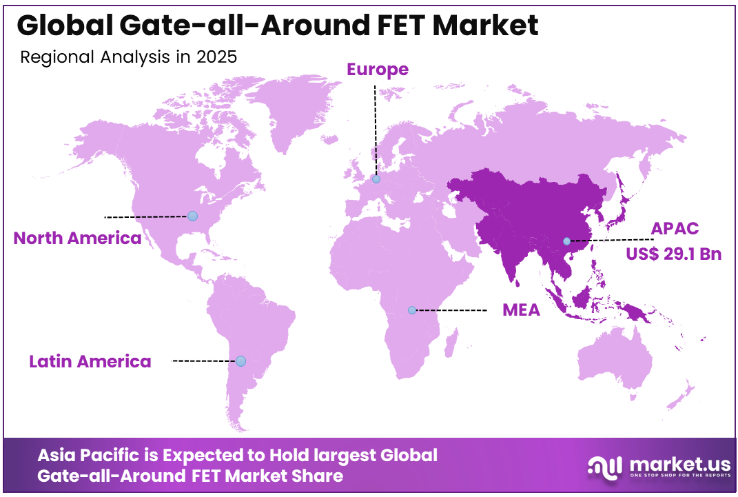
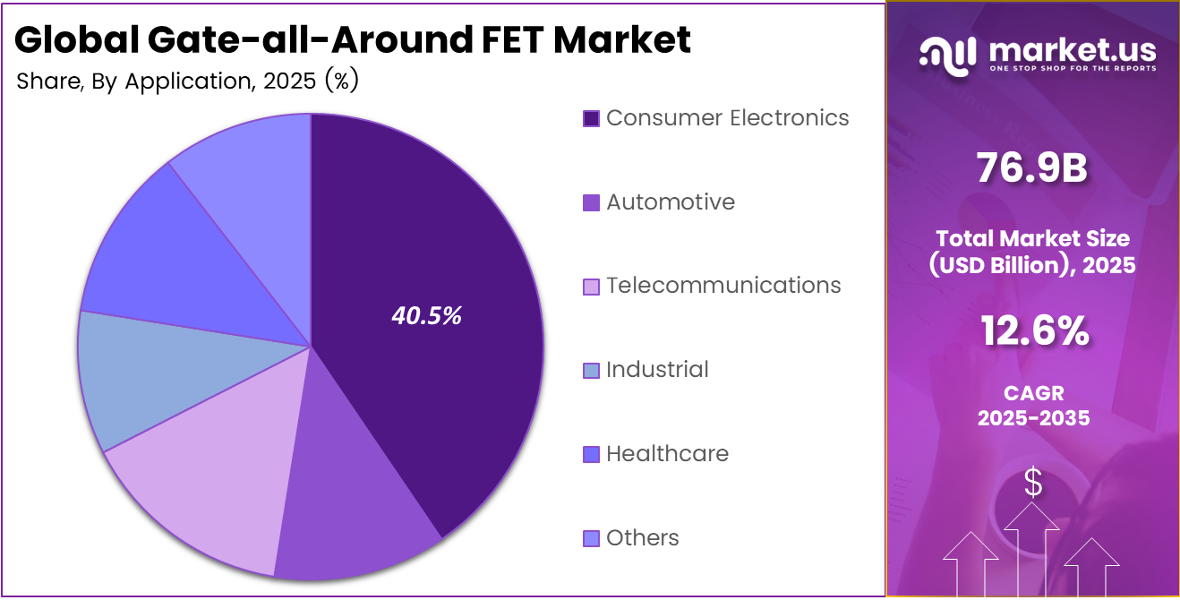
The Global Gate-all-Around FET Market size is expected to be worth around USD 251.9 billion by 2035, from USD 76.9 billion in 2025, growing at a CAGR of 12.6% during the forecast period from 2025 to 2035. Asia Pacific held a dominant market position, capturing more than a 37.9% share, holding USD 29.1 billion in revenue.
Gate-all-Around FET refers to an advanced transistor structure where the gate surrounds the channel from all sides to control current flow more effectively. This design helps reduce power leakage, improve switching performance, and support smaller chip nodes. It is used in next-generation semiconductors for AI, mobile, and high-performance computing applications. 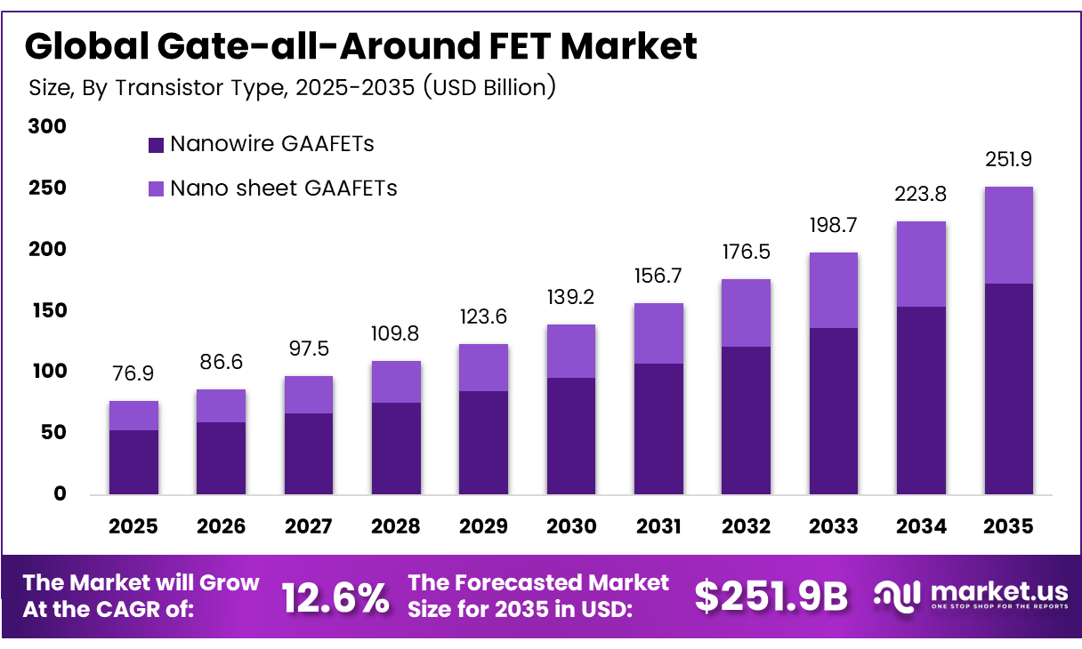
Top driving factors include the push to reduce power use per operation in AI and data center chips. Demand is also supported by the need to scale beyond roughly 5 nanometers, where FinFET faces limits. Power efficiency gains above 30% in some nodes help chip designers manage heat in compact and high-performance systems.
The market for Gate-all-Around FET is driven by the need for smaller, faster, and more power-efficient chips. As traditional transistor designs face scaling limits, GAAFET provides better current control and lower leakage. Its adoption is supported by rising demand for AI processors, smartphones, data centers, electric vehicles, and connected devices that require high performance within compact chip designs.
Demand Analysis is strengthening as more than one-third of leading chip makers are moving development roadmaps toward gate all around platforms for next-generation logic. Connected devices, electric vehicles, and always-on edge systems are adding further demand, as each advanced chip can hold billions of these transistors on a single die.
For instance, in March 2025, Synopsys released updated TCAD and EDA platforms with calibrated models for nanosheet and Gate-all-Around devices down to 2 nm. The tools allow foundries and fabless companies to co-optimize GAA device physics, standard-cell libraries, and 3D packaging, shortening design cycles for AI, 5G, and automotive chips.
Key Takeaway
- In 2025, the Nanowire GAAFETs segment held a dominant market position, capturing a 68.7% share of the Global Gate-all-Around FET Market.
- In 2025, the Consumer Electronics segment held a dominant market position, capturing a 40.5% share of the Global Gate-all-Around FET Market.
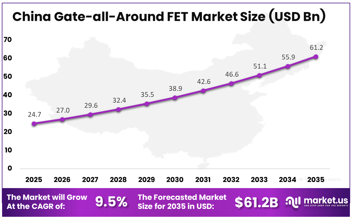
- The China Gate-all-Around FET Market was valued at USD 24.7 Billion in 2025, with a robust CAGR of 9.5%.
- In 2025, the Asia Pacific held a dominant market position in the Global Gate-all-Around FET Market, capturing more than a 37.9% share.
Role of Generative AI
Generative AI is helping GAA device teams test more design options before final production. It supports faster comparison of channel shapes, materials, and power behavior, reducing dependence on slow manual simulation cycles. This is useful as advanced chip design costs continue to rise sharply at leading nodes.
It also supports better design productivity in manufacturing and product engineering. Generative design tools can shorten physical product design cycles, while expert review remains important for accuracy and safety. In GAA development, this can help teams reduce trial work and focus resources on the most practical device structures.
Investment and Business Benefits
Investment Opportunities are emerging across the value chain, including nanowire materials, high-k dielectrics, and inspection tools that can image features well below 10 nanometers. Growth potential is also seen in design IP, compact models, and specialty fabs serving low-volume but high-value sectors such as aerospace, defense, and medical electronics.
Business Benefits for adopters include stronger performance per watt, longer product life at advanced nodes, and better alignment with energy-efficient electronics rules. Early movers can spread design and tooling costs across multiple product generations. This improves capital productivity and supports stronger competitiveness in advanced semiconductor portfolios.
Regional Analysis
In 2025, the Asia Pacific held a dominant market position in the Global Gate-all-Around FET Market, capturing more than a 37.9% share, holding USD 29.1 billion in revenue. This dominance is due to the Asia Pacific’s strong semiconductor manufacturing base, large foundry ecosystem, and rising investment in advanced chip technologies. The region benefits from high demand for smartphones, AI processors, electric vehicles, and connected devices. Countries such as China, South Korea, Taiwan, and Japan are also supporting next-generation node development, making Gate-all-Around FET adoption important for power-efficient and high-performance chip production.
For instance, in March 2025, Samsung Electronics boosted Asia-Pacific leadership in GAAFET by securing about USD 8.5 billion in Korean incentives dedicated to scaling its gate-all-around process nodes and improving yields for 3 nm and future 2 nm lines. The funding strengthens Samsung’s role as a regional anchor for advanced AI and HPC chips.
China Gate-all-Around FET Market Size
The market for Gate-all-Around FET within China is growing tremendously and is currently valued at USD 24.7 billion; the market has a projected CAGR of 9.5%. The market is growing due to China’s strong focus on advanced semiconductor manufacturing, high demand for AI chips, and rising investment in domestic chip capabilities. Growth is also supported by expanding consumer electronics, electric vehicles, cloud computing, and 5G infrastructure. As chip designs move toward smaller and more power-efficient nodes, Gate-all-Around FET technology is becoming important for improving performance, reducing leakage, and supporting next-generation processors.
For instance, in February 2024, SMIC reportedly advanced its 5 nm-class and exploratory Gate-all-Around transistor research to support Huawei’s next-generation AI and 5G chips, underscoring China’s push to localize advanced logic manufacturing under export controls while positioning SMIC as the country’s central foundry player in emerging GAAFET-based nodes.
Key Regions and Countries
North America
- US
- Canada
Europe
- Germany
- France
- The UK
- Spain
- Italy
- Russia
- Netherlands
- Rest of Europe
Asia Pacific
- China
- Japan
- South Korea
- India
- Australia
- Singapore
- Thailand
- Vietnam
- Rest of APAC
Latin America
- Brazil
- Mexico
- Rest of Latin America
Middle East & Africa
- South Africa
- Saudi Arabia
- UAE
- Rest of MEA
Transistor Type Analysis
In 2025, the Nanowire GAAFETs segment held a dominant market position, capturing a 68.7% share of the Global Gate-all-Around FET Market. This dominance is due to the strong gate control offered by nanowire GAAFETs, where the gate surrounds the channel from all sides. This structure helps reduce leakage, improve switching behavior, and support continued scaling as traditional transistor designs face limits at smaller nodes.
Nanowire GAAFETs are also preferred because they provide better control over current flow in compact chip designs. Their structure supports lower power use and reliable performance, making them suitable for advanced processors, mobile chips, and high-density logic applications that require stable operation.
For instance, in December 2025, TSMC confirmed that its N2 platform entered volume production with a GAAFET-based architecture, marking its first mainstream move away from FinFET at 2 nm. By putting GAA into a high-volume logic process, TSMC makes nanowire-style devices more accessible for major CPU and GPU designers planning their next-generation chips.
Application Analysis
In 2025, the Consumer Electronics segment held a dominant market position, capturing a 40.5% share of the Global Gate-all-Around FET Market. This dominance is due to the rising need for smaller, faster, and more energy-efficient chips in consumer devices. Smartphones, tablets, wearables, and connected home products require processors that can deliver strong performance while controlling heat and battery usage in compact form factors.
Consumer electronics brands are adopting advanced transistor designs to support better graphics, AI features, multitasking, and longer battery life. GAAFET technology helps chip designers improve power efficiency and performance, which makes it important for next-generation devices with higher processing needs and limited physical space.
For instance, in October 2024, Intel’s roadmap linking RibbonFET and PowerVia to future client processors indicates that GAAFETs will underpin upcoming PCs and thin-and-light laptops. As these chips move into consumer systems, users benefit from faster performance within similar power envelopes, which is crucial for fanless designs and longer unplugged use.
Key Market Segments
By Transistor Type
- Nano sheet GAAFETs
- Nanowire GAAFETs
By Application
- Consumer Electronics
- Automotive
- Telecommunications
- Industrial
- Healthcare
- Others
Emerging Trends
One major trend is the movement from early nanowire concepts toward nanosheet GAA structures. Nanosheets provide a stronger drive current while keeping good electrostatic control. This makes them suitable for AI, mobile, and high-performance computing chips that need both speed and energy efficiency.
Architecture development is also widening across the forked and multi-bridge channel designs. These structures are being studied to balance performance, leakage, and footprint for different workloads. Wider nanosheets can support higher performance, while narrower sheets can help compact and low-power designs.
Growth Factors
Growth is mainly supported by AI and data-centric computing, where chips need dense logic and better power control. GAA designs help extend scaling as FinFET structures become harder to optimize at very small nodes. This makes the technology important for advanced processors and edge devices.
Another growth factor is the rising cost and complexity of traditional chip design. Advanced-node design cost is estimated to move toward $1 billion for the most complex chips, creating pressure to improve design efficiency. GAA offers a path to extend performance gains without depending only on lithography improvements.
Market Dynamics
Drivers - Transition to Next-Generation Transistor Architecture
The shift toward Gate-all-Around FET is being driven by the need for stronger transistor control at smaller chip nodes. As older architectures face scaling limits, GAAFET helps reduce leakage, improve switching behavior, and support higher device density in advanced logic chips.
This transition also supports better power efficiency in AI processors, mobile chips, and high-performance computing platforms. By surrounding the channel from all sides, the gate provides improved current control, making the technology suitable for next-generation semiconductor designs that require compact size and reliable performance.
For instance, in February 2026, Samsung highlighted progress on its 2 nm GAAFET node, stating that its Ribbon-style MBCFET design will underpin next-generation mobile and AI system-on-chips, with better performance per watt than earlier 3 nm implementations and a wider design window for customers moving beyond FinFET platforms.
Restraint - High Fabrication Cost
High fabrication cost remains a major restraint for the Gate-all-Around FET market. The process requires advanced lithography, precise material deposition, selective etching, and strict defect control, which increases production expenses compared with mature transistor technologies.
Smaller semiconductor companies may find adoption difficult because the technology needs expensive tools, skilled engineers, and long process qualification cycles. These cost pressures can slow wider commercialization, especially in applications where buyers are highly sensitive to chip pricing.
For instance, in January 2026, Applied Materials reported strong growth in advanced wafer fabrication systems, but also noted that customers face steep capital intensity as they invest in new tools for GAAFET and 3D NAND, which raises the overall cost of ramping advanced-node fabs and makes ROI a central concern for chipmakers.
Opportunities - AI and Advanced Computing Demand
AI and advanced computing demand create a strong opportunity for the Gate-all-Around FET market. These workloads need chips that can deliver high performance while using less power. GAAFET technology supports this need by improving current control and enabling denser transistor placement.
The opportunity is also supported by rising demand for data centers, edge AI, smartphones, and connected devices. As computing systems become more power sensitive, GAAFET can help chip designers balance speed, energy use, and heat control in next-generation processors.
For instance, in May 2025, GlobalFoundries outlined a roadmap focused on specialized and power-efficient platforms rather than chasing the smallest geometry, stressing that growing AI and edge workloads still create demand for optimized RF, embedded, and low-power processes where the company can serve AI-enabled devices without adopting full GAAFET scaling.
Challenges - Complex Manufacturing Process
Complex manufacturing remains a key challenge for the Gate-all-Around FET market. The structure requires careful formation of nanosheets or nanowires, along with accurate gate placement around the channel. This makes production more difficult than earlier transistor technologies.
Process variation is another concern because tiny changes in shape or material quality can affect device performance. Manufacturers must improve yield, reliability, and design validation before large-scale adoption becomes easier. This creates pressure on engineering teams across the semiconductor value chain.
For instance, in February 2022, Lam Research detailed selective etch solutions for GAA inner spacers and nanosheet release, achieving highly selective removal of SiGe without damaging surrounding layers. The company’s atomic-level etch and ALE approaches demonstrate that precise process control is essential for managing the complexity of GAAFET manufacturing and maintaining yields.
Key Players Analysis
One of the leading players in July 2025, Lam Research expanded its atomic layer deposition and etch solutions tailored to GAA device integration, focusing on precise nanosheet gate-stack and spacer formation. These process tools are essential to achieving tight dimensional control in stacked channels, enabling higher drive current and lower leakage for sub-3 nm nodes.
Top Key Players in the Market
- Samsung Electronics
- Taiwan Semiconductor Manufacturing Company (TSMC)
- Intel Corporation
- Applied Materials, Inc.
- ASML Holding N.V.
- Lam Research Corporation
- GlobalFoundries
- IBM Corporation
- SK Hynix Inc.
- Synopsys, Inc.
- ABB Group
- IXYS Corporation
- Renesas Electronics Corporation
- Fairchild Semiconductor International, Inc.
Recent Developments
- In May 2025, TSMC confirmed that its 2 nm N2 GAA node remains on track for risk production in 2025, with volume ramp expected in 2026. The nanosheet-based architecture will replace FinFETs at advanced nodes, anchoring TSMC’s roadmap for AI accelerators, data-center CPUs, and flagship smartphone processors.
- In April 2025, Intel reiterated that its RibbonFET Gate-all-Around technology will debut at the 20A and 18A nodes, designed with backside power delivery (PowerVia) to boost performance per watt. These GAA nodes are central to Intel’s plan to regain process leadership and attract external foundry customers in AI and cloud markets.
- In January 2025, GlobalFoundries outlined a technology partnership strategy to bring selective Gate-all-Around capabilities into future specialty and RF platforms, rather than chasing leading-edge logic. The foundry plans to selectively leverage GAA features for ultra-low-power and high-reliability applications in the automotive, IoT, and defense markets.
Report Scope
| Report Features | Description |
|---|---|
| Market Value (2025) | USD 76.9 Billion |
| Forecast Revenue (2035) | USD 251.9 Billion |
| CAGR (2026-2035) | 12.6% |
| Base Year for Estimation | 2025 |
| Historic Period | 2020-2024 |
| Forecast Period | 2026-2035 |
| Report Coverage | Revenue Forecast, Market Dynamics, Competitive Landscape, Recent Developments |
| Segments Covered | By Transistor Type (Nano sheet GAAFETs, Nanowire GAAFETs), By Application (Consumer Electronics, Automotive, Telecommunications, Industrial, Healthcare, Others) |
| Regional Analysis | North America (US and Canada), Europe (Germany, France, The UK, Spain, Italy, and Rest of Europe), Asia Pacific (China, Japan, South Korea, India, Australia, and Rest of APAC), Latin America (Brazil, Mexico, and Rest of Latin America), Middle East & Africa (GCC, South Africa, and Rest of MEA) |
| Competitive Landscape | Samsung Electronics, Taiwan Semiconductor Manufacturing Company (TSMC), Intel Corporation, Applied Materials, Inc., ASML Holding N.V., Lam Research Corporation, GlobalFoundries, IBM Corporation, SK Hynix Inc., Synopsys, Inc., ABB Group, IXYS Corporation, Renesas Electronics Corporation, Fairchild Semiconductor International, Inc. |
| Customization Scope | Customization at the segment and region/country levels will be provided. Moreover, customization can be tailored to the requirements. |
| Purchase Options | We have three licenses to opt for: Single User License, Multi-User License (Up to 5 Users), Corporate Use License (Unlimited Users and Printable PDF) |