Global Molded Underfill Material Market Size, Share Analysis Report By Technology (Dynamic Mechanic Analyzer, Thermal Mechanical Analyzer, Thermo-gravimetrical Analyzer, and Differential Scanning Calorimeter), By Application (Flip Chip Packaging, Ball Grid Array, Chip Scale Packaging, Land Grid Array, Wafer-Level Packaging, and Others), By Region and Companies - Industry Segment Outlook, Market Assessment, Competition Scenario, Trends and Forecast 2025-2034
- Published date: Jan 2025
- Report ID: 172819
- Number of Pages: 312
- Format:
-
keyboard_arrow_up
Quick Navigation
Report Overview
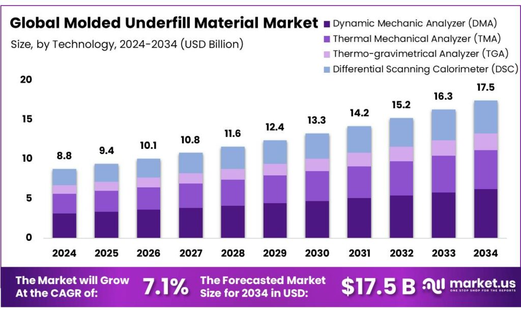
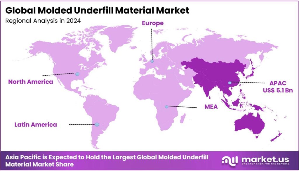
The Global Molded Underfill Material Market size is expected to be worth around USD 17.5 Billion by 2034, from USD 8.8 Billion in 2024, growing at a CAGR of 7.1% during the forecast period from 2025 to 2034. In 2024 Asia Pacific held a dominant market position, capturing more than a 58.2% share, holding USD 5.1 Billion in revenue.
Molded Underfill (MUF) material is a specialized epoxy resin used in semiconductor packaging to fill the gap between a microchip and its substrate, providing structural support, thermal management, and protection for solder joints, all while streamlining production by combining the underfill and overmolding processes into one, leading to lower costs, faster manufacturing, and smaller chip sizes. Its market is primarily driven by the growing demand for advanced semiconductor packaging solutions, particularly as the electronics industry focuses on miniaturization and high-performance devices.
- According to the Semiconductor Industry Association (SIA), the global semiconductor sales were US$72.7 billion during the month of October 2025, an increase of 4.7% compared to the September 2025 total of US$69.5 billion and 27.2% more than the October 2024 total of US$57.2 billion. As the semiconductor industry grows, it creates opportunities for advanced semiconductor technologies, such as molded underfill material.
Key factors such as the rise of flip chip packaging (FCP), automotive electrification, and the shift towards wide bandgap (WBG) semiconductors for power electronics have boosted the demand for these materials. Molded underfills are essential for protecting sensitive semiconductor components from thermal and mechanical stress, enhancing device durability, and ensuring reliability in applications ranging from consumer electronics to electric vehicles and data centers.
However, challenges such as high R&D costs and complex manufacturing processes continue to influence supply chains and operational costs. Despite these hurdles, the market continues to evolve, driven by the demand for more efficient and resilient packaging solutions.
Key Takeaways
- The global molded underfill material market was valued at USD 8.8 billion in 2024.
- The global molded underfill material market is projected to grow at a CAGR of 7.1% and is estimated to reach USD 17.5 billion by 2034.
- Based on the technology, the dynamic mechanical analyzer (DMA) dominated the molded underfill material market, with a market share of around 35.6%.
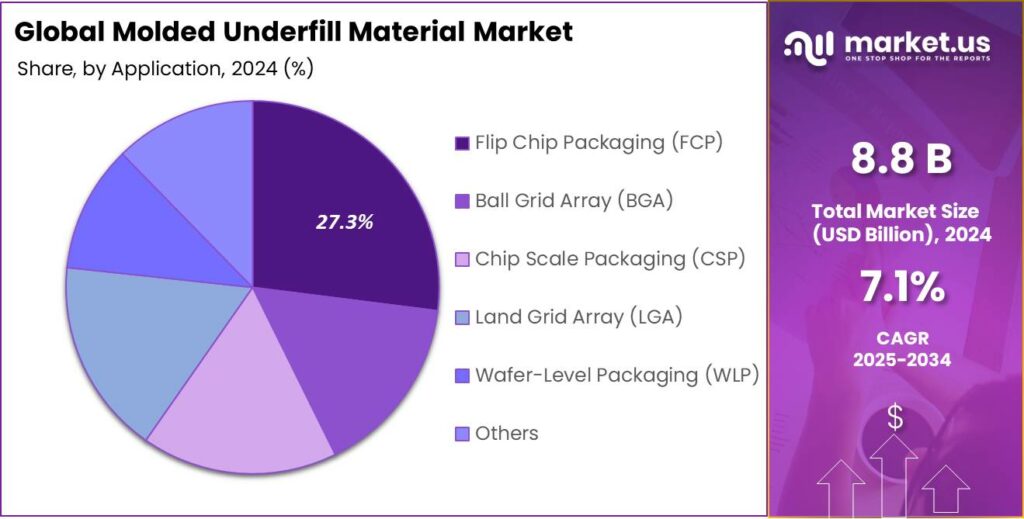
- Among the applications of molded underfill material, the flip chip packaging (FCP) held a major share in the market, 27.3% of the market share.
- In 2024, the APAC was the most dominant region in the molded underfill material market, accounting for around 58.2% of the total global consumption.
Technology Analysis
Dynamic Mechanic Analyzer (DMA) Held the Largest Share in the Market.
The molded underfill material market is segmented based on the technology into dynamic mechanical analyzer (DMA), thermal mechanical analyzer (TMA), thermo-gravimetrical analyzer (TGA), and differential scanning calorimeter (DSC). The dynamic mechanical analyzer (DMA) dominated the market, comprising around 35.6% of the market share, due to DMA’s ability to assess the viscoelastic properties of underfill materials under real-world conditions.
DMA is particularly effective in evaluating how materials respond to varying temperatures and mechanical stresses, which is crucial for molded underfills that must endure thermal cycling and mechanical load in electronic devices. Unlike TMA, TGA, or DSC, which mainly focus on material composition or thermal properties, DMA provides a comprehensive understanding of the material’s performance in operational environments, making it more relevant for manufacturers aiming to ensure reliability and durability in high-performance semiconductor packages. This precise evaluation of mechanical integrity directly impacts product quality and market demand.
Application Analysis
The Molded Underfill Material Was Mostly Utilized in the Flip Chip Packaging (FCP).
Based on the applications of molded underfill material, the market is divided into flip chip packaging (FCP), ball grid array (BGA), chip scale packaging (CSP), land grid array (LGA), wafer-level packaging (WLP), and others. The flip chip packaging (FCP) dominated the market, with a market share of 27.3%, due to its widespread adoption in high-performance and miniaturized electronic devices. FCP offers superior electrical performance and heat dissipation, which are critical in applications such as smartphones, high-speed computing, and advanced automotive electronics.
The use of molded underfill in FCP is essential for enhancing mechanical stability and protecting delicate semiconductor components from thermal and mechanical stress. In contrast, while ball grid array (BGA), chip scale packaging (CSP), land grid array (LGA), and wafer-level packaging (WLP) utilize underfill materials, they do not require the same level of robust protection against thermal cycling and stress, making the demand for molded underfill materials in these packaging types comparatively lower. The increasing demand for smaller and more powerful devices drives the higher revenue generated from FCP.
Key Market Segments
By Technology
- Dynamic Mechanic Analyzer (DMA)
- Thermal Mechanical Analyzer (TMA)
- Thermo-gravimetrical Analyzer (TGA)
- Differential Scanning Calorimeter (DSC)
By Application
- Flip Chip Packaging (FCP)
- Ball Grid Array (BGA)
- Chip Scale Packaging (CSP)
- Land Grid Array (LGA)
- Wafer-Level Packaging (WLP)
- Others
Drivers
Semiconductor Miniaturization & Integration Drives the Molded Underfill Material Market.
The semiconductor industry’s ongoing trend toward miniaturization and integration significantly drives the demand for molded underfill materials. As devices continue to shrink in size, the complexity of semiconductor packaging increases, necessitating advanced materials that offer high reliability and superior performance. Molded underfill materials, which protect semiconductor components from thermal and mechanical stress, are crucial in ensuring the longevity and functionality of smaller, more compact chips.
The rise of consumer electronics, automotive applications, and wearable devices further accelerates this demand, as these sectors require increasingly efficient and robust semiconductor components. For instance, in advanced packaging technologies such as system-in-package (SiP) and chip-on-board (COB), molded underfill plays a critical role in providing protection against environmental factors and enhancing thermal conductivity. As semiconductor nodes continue to move below 10 nm, the demand for high-performance underfill materials that can withstand tighter tolerances and higher heat dissipation becomes paramount.
Restraints
High R&D Costs and Complex Manufacturing Pose a Challenge to the Molded Underfill Material Market.
The molded underfill material market faces significant challenges due to the high research and development (R&D) costs and the complexity of manufacturing processes. Developing advanced underfill materials that meet the stringent requirements of modern semiconductor packaging demands substantial investment in R&D. This includes extensive testing for properties such as thermal conductivity, adhesion strength, and moisture resistance, which are essential for ensuring the reliability of the final product.
Furthermore, the production of molded underfill materials involves intricate manufacturing techniques, including precise molding and curing processes, which require specialized equipment and highly skilled labor. These complexities often lead to higher operational costs and longer production timelines. For instance, as semiconductor manufacturers push toward smaller chip sizes and more integrated solutions, the formulations for underfill materials must be continuously adjusted to accommodate tighter spaces and higher thermal loads. Consequently, the increased technical demands and production hurdles can limit the scalability and profitability of molded underfill solutions.
Opportunity
Automotive Electrification and Demand for High-Performance Computing (HPC) Create Opportunities in the Molded Underfill Material Market.
The growing trend of automotive electrification and the increasing demand for high-performance computing (HPC) are creating significant opportunities for the molded underfill material market. According to the International Energy Agency (IEA), the electric car sales exceeded 17 million globally in 2024, reaching a sales share of more than 20%. As electric vehicles (EVs) become more mainstream, there is an intensified demand for advanced semiconductor components that are compact and capable of handling high thermal and electrical loads.
Molded underfill materials play a crucial role in these applications by providing protection and ensuring the durability of semiconductor packages used in power management systems, battery management units, and other electronic components within EVs. Similarly, the HPC sector, driven by the rise of artificial intelligence (AI), cloud computing, and data centers, requires robust semiconductor packaging solutions to manage the heat generated by increasingly powerful processors.
- For instance, in data center servers and AI accelerators, molded underfill helps mitigate the risks of mechanical stress and thermal cycling, ensuring the reliability and efficiency of high-performance chips. Globally, there are over 12,000 operational data centers, with the U.S. accounting for 45% of all facilities worldwide.
Trends
Adoption of the WBG (Wide Bandgap) Semiconductors for Power Electronics.
The application of molded underfill materials in wide bandgap (WBG) semiconductor devices for power electronics is an emerging trend within the semiconductor industry. WBG semiconductors, such as silicon carbide (SiC) and gallium nitride (GaN), are gaining traction due to their superior efficiency, high thermal conductivity, and ability to operate at higher voltages and temperatures compared to traditional silicon-based semiconductors. These properties make them ideal for power electronics applications in industries such as automotive, renewable energy, and industrial automation.
However, WBG devices face challenges related to thermal stress and mechanical reliability, due to their higher power densities and operating temperatures. Molded underfill materials address these challenges by providing robust thermal management, mechanical protection, and moisture resistance, thereby enhancing the longevity and performance of WBG semiconductor devices. For instance, in electric vehicle power inverters and renewable energy systems, the use of underfill materials ensures that WBG components can withstand the rigorous thermal cycles, improving the overall efficiency and durability of these systems.
Geopolitical Impact Analysis
Geopolitical Tensions Are Impacting the Molded Underfill Material Market by Shifting Trade Flows.
The geopolitical tensions have had a notable impact on the molded underfill material market, affecting supply chains, manufacturing capabilities, and global trade dynamics. For instance, disruptions in semiconductor production and raw material supply, particularly in regions such as East Asia and Eastern Europe, have led to delays and increased costs for manufacturers of underfill materials.
The ongoing trade restrictions and tariffs, particularly between the major economies of the U.S. and China, have further complicated access to essential raw materials such as resins, silica, and other specialized compounds used in the formulation of molded underfill materials. In addition, these geopolitical challenges have caused a shift in sourcing strategies, with companies seeking to diversify their supplier bases to mitigate risks, thus increasing the complexity of procurement and raising logistics costs.
Regional Analysis
Asia Pacific Held the Largest Share of the Global Molded Underfill Material Market.
In 2024, the Asia Pacific dominated the global molded underfill material market, holding about 58.2% of the total global consumption. The region has consistently held the largest share of the global molded underfill material market, driven by the region’s dominance in semiconductor manufacturing and assembly. Countries such as China, South Korea, Japan, and Taiwan are global leaders in electronics and semiconductor production, which significantly boosts the demand for molded underfill materials.
For instance, Taiwan, where major foundries such as Taiwan Semiconductor Manufacturing Company (TSMC) reside, plays a pivotal role in the production of advanced semiconductors used in consumer electronics, automotive systems, and telecommunications.
In 2023, TSMC had emerged as the global leader in semiconductor manufacturing, commanding 65% of the global foundry market, which makes virtually all advanced AI chips for companies such as Nvidia and Google. Additionally, the rapid expansion of industries such as EVs and consumer electronics in Asia contributes to the trend. Furthermore, cost-effective manufacturing and the availability of skilled labor in the region further solidify the leadership of region in this market.
Key Regions and Countries
- North America
- The US
- Canada
- Europe
- Germany
- France
- The UK
- Spain
- Italy
- Russia & CIS
- Rest of Europe
- APAC
- China
- Japan
- South Korea
- India
- ASEAN
- Rest of APAC
- Latin America
- Brazil
- Mexico
- Rest of Latin America
- Middle East & Africa
- GCC
- South Africa
- Rest of MEA
Key Players Analysis
Companies in the molded underfill material market focus on several strategic activities to expand their market reach and stay ahead of the competition. The companies focus on investing heavily in research and development (R&D) to create innovative, high-performance materials that meet the evolving demands of industries such as consumer electronics, automotive, and power electronics.
Similarly, these players emphasize collaborating with semiconductor manufacturers and packaging service providers to develop tailored solutions for specific applications, enhancing their product offerings. Additionally, the companies focus on expanding their production capacity in regions with strong semiconductor manufacturing hubs, particularly in the Asia Pacific. Furthermore, there is an emphasis on strategic acquisitions and partnerships to access new technologies, strengthen their market position, and broaden their product portfolios.
The Major Players in The Industry
- Panasonic Holdings Corporation
- Fujitsu Ltd.
- Henkel AG & Co. KGaA
- Parker-Hannifin Corp.
- Nordson Corp.
- American Iron & Metal (AIM)
- Namics Corporation
- Epoxy Technology Inc.
- Master Bond Inc.
- Indium Corporation
- SK Hynix
- Won Chemical Co., Ltd.
Key Development
- In August 2025, Indium Corporation, a globally recognized refiner, smelter, manufacturer, and supplier of advanced materials, announced the launch of WS-910 Flip-Chip Flux, a water-soluble dipping flux engineered to address the performance demands of next-generation semiconductor devices.
- In September 2025, SK Hynix completed the development of HBM4, the 6th generation high-bandwidth memory for ultra-high-performance artificial intelligence, and established the world’s first mass production system, with its proprietary advanced MR-MUF (Mass Reflow-Molded Underfill) process.
Report Scope
Report Features Description Market Value (2024) USD 8.8 Bn Forecast Revenue (2034) USD 17.5 Bn CAGR (2025-2034) 7.1% Base Year for Estimation 2024 Historic Period 2020-2023 Forecast Period 2025-2034 Report Coverage Revenue Forecast, Market Dynamics, Competitive Landscape, Recent Developments Segments Covered By Technology (Dynamic Mechanic Analyzer (DMA), Thermal Mechanical Analyzer (TMA), Thermo-gravimetrical Analyzer (TGA), and Differential Scanning Calorimeter (DSC)), By Application (Flip Chip Packaging (FCP), Ball Grid Array (BGA), Chip Scale Packaging (CSP), Land Grid Array (LGA), Wafer-Level Packaging (WLP), and Others) Regional Analysis North America – The US & Canada; Europe – Germany, France, The UK, Spain, Italy, Russia & CIS, Rest of Europe; APAC– China, Japan, South Korea, India, ASEAN & Rest of APAC; Latin America– Brazil, Mexico & Rest of Latin America; Middle East & Africa– GCC, South Africa, & Rest of MEA Competitive Landscape Panasonic Holdings Corporation, Fujitsu Ltd., Henkel AG & Co. KGaA, Parker-Hannifin Corp., Nordson Corp., American Iron & Metal (AIM), Namics Corporation, Epoxy Technology Inc., Master Bond Inc., Indium Corporation, SK Hynix, Won Chemical Co. Ltd., and Other Players. Customization Scope Customization for segments, region/country-level will be provided. Moreover, additional customization can be done based on the requirements. Purchase Options We have three licenses to opt for: Single User License, Multi-User License (Up to 5 Users), Corporate Use License (Unlimited Users and Printable PDF)  Molded Underfill Material MarketPublished date: Jan 2025add_shopping_cartBuy Now get_appDownload Sample
 -
-
- Panasonic Holdings Corporation
- Fujitsu Ltd.
- Henkel AG & Co. KGaA
- Parker-Hannifin Corp.
- Nordson Corp.
- American Iron & Metal (AIM)
- Namics Corporation
- Epoxy Technology Inc.
- Master Bond Inc.
- Indium Corporation
- SK Hynix
- Won Chemical Co., Ltd.
Our Clients
- 172819
- Jan 2025