Quick Navigation
Report Overview
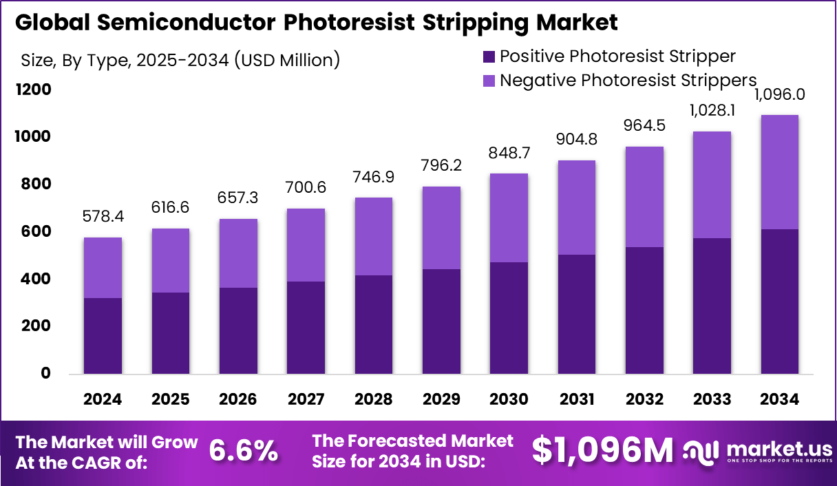
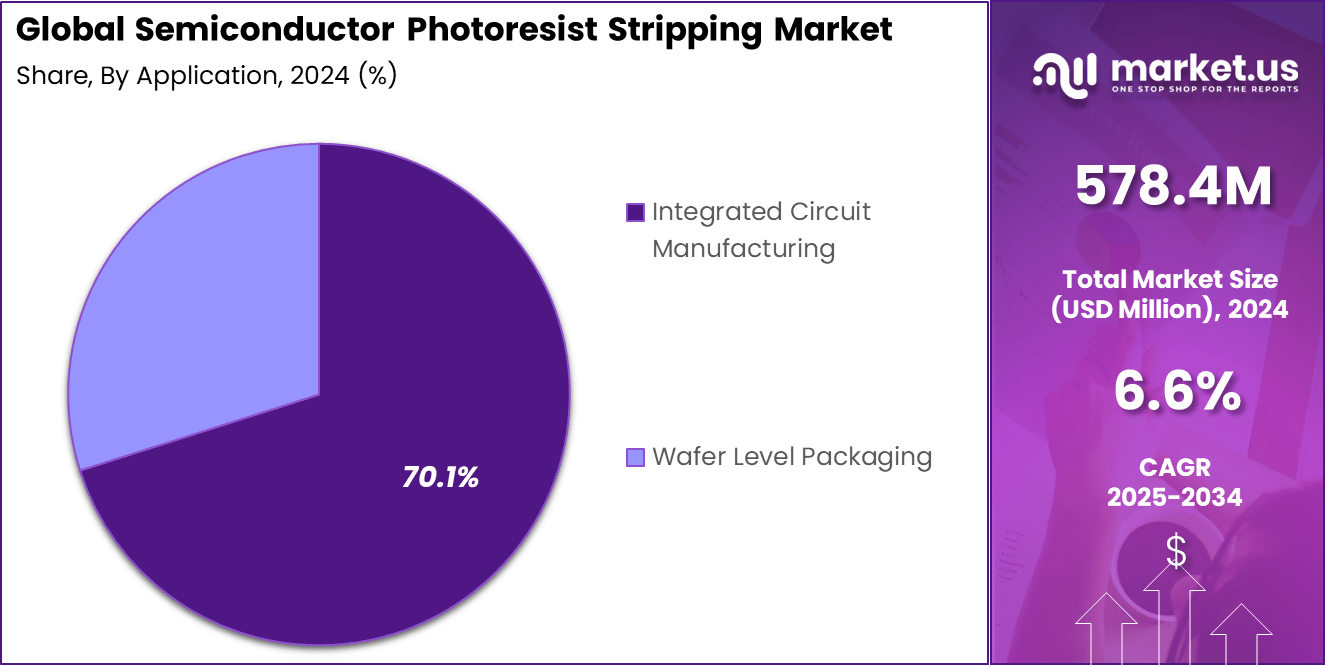
The Global Semiconductor Photoresist Stripping Market size is expected to be worth around USD 1,096 Million By 2034, from USD 578.4 Million in 2024, growing at a CAGR of 6.6% during the forecast period from 2025 to 2034. In 2024, APAC held a dominant market position, capturing more than a 45% share, holding USD 260.28 Million revenue.
The semiconductor photoresist stripping market is an integral part of the semiconductor manufacturing industry, primarily driven by the necessity for high precision and purity in semiconductor device fabrication. The market is characterized by a continual demand for innovative solutions that enhance efficiency and reduce contamination risks during the stripping process.
The primary drivers of the semiconductor photoresist stripping market include the increasing complexity of semiconductor device architectures and the growing demand for smaller, more efficient devices. As devices shrink in size, the precision required in the photoresist stripping process increases, thereby pushing for advancements in stripping technology.
The need for higher throughput and lower contamination in manufacturing environments also significantly drives the market. There is a notable shift towards dry stripping methods, especially plasma-based techniques, due to their ability to provide high precision and minimal contamination. These technologies are becoming more popular as they meet the stringent cleanliness requirements of advanced semiconductor fabrication processes.
The adoption of advanced stripping technologies is primarily due to their efficiency and the lower environmental impact compared to traditional wet chemical methods. Plasma stripping, for instance, does not use large volumes of chemicals and generates less waste, aligning with the industry’s move towards greener manufacturing practices.
According to Market.us, The semiconductor market is projected to grow from USD 530 billion in 2023 to approximately USD 996 billion by 2033, reflecting a compound annual growth rate (CAGR) of 6.5% during the forecast period from 2024 to 2033. In 2023, the Asia-Pacific (APAC) region held a dominant market position, capturing more than a 63.91% share, equating to USD 388.7 billion in revenue.
The demand for semiconductor photoresist stripping solutions is closely tied to the semiconductor industry’s production cycles. With the increasing production of electronic devices such as smartphones, tablets, and other smart technologies, there is a robust demand for effective and efficient stripping solutions that can support large-scale manufacturing.
The market is witnessing a trend towards automation and the integration of smart technologies in stripping equipment. This not only enhances precision but also allows for better control and monitoring of the process, reducing human error and improving overall yield rates in semiconductor production.
Key Takeaways
- The global semiconductor photoresist stripping market is projected to reach a valuation of USD 1,096 million by 2034, up from USD 578.4 million in 2024. This growth reflects a Compound Annual Growth Rate (CAGR) of 6.6% during the forecast period from 2025 to 2034.
- In 2024, the Asia-Pacific (APAC) region held a leading position in the market. It accounted for more than 45% of the global revenue, generating approximately USD 260.28 million.
- The Positive Photoresist Stripper segment showed significant traction in 2024. It contributed to more than 56% of the total market share.
- In terms of application, the Integrated Circuit (IC) Manufacturing segment dominated the market landscape. In 2024, it accounted for over 70.1% of the global revenue share.
Analysts’ Viewpoint
For businesses, efficient photoresist stripping technologies can lead to reduced operational costs, improved production efficiency, and lower defect rates in semiconductor manufacturing. These benefits contribute to a competitive advantage in the fast-paced semiconductor industry.
Recent advancements include the development of low-power, high-efficiency plasma systems for dry stripping that offer precise control over the stripping process, essential for maintaining the integrity of underlying materials in advanced semiconductor devices.
The regulatory environment for semiconductor manufacturing, including photoresist stripping, is increasingly focusing on reducing solvent emissions and hazardous waste. Regulations such as REACH (Registration, Evaluation, Authorization, and Restriction of Chemicals) in Europe and similar standards globally are pushing manufacturers towards adopting safer and more sustainable practices.
Impact of AI
The integration of Artificial Intelligence (AI) in the semiconductor photoresist stripping processes is transforming this industry segment by enhancing efficiency, precision, and sustainability. The following points encapsulate the impact of AI on the semiconductor photoresist stripping sector:
- Optimization of Process Parameters: AI technologies such as Machine Learning (ML) and Reinforcement Learning (RL) are pivotal in analyzing and optimizing stripping processes. They enable real-time adjustments to chemical concentrations, flow rates, and temperatures, which are critical for maximizing efficiency and minimizing waste during the stripping process.
- Enhanced Quality Control and Defect Detection: AI-driven systems incorporate advanced imaging and diagnostic tools that facilitate real-time quality assessment and defect detection. This integration not only helps in maintaining high standards of manufacturing precision but also significantly reduces the cycle times for stripping processes.
- Sustainability and Environmental Compliance: AI applications extend to monitoring and managing the environmental impact of the stripping processes. For instance, AI can optimize the lifecycle of chemicals used in stripping, thereby promoting recycling and reducing waste. Furthermore, AI aids in achieving energy efficiency, particularly in plasma stripping processes, by identifying and implementing energy-saving measures
- Future Prospects and Innovations: The ongoing advancements in AI are expected to lead towards more autonomous stripping systems capable of dynamic adaptations. These systems are likely to address a wide range of contamination scenarios, which will be crucial as device geometries continue to shrink and the complexity of semiconductor devices increases.
APAC Market Size
In 2024, APAC held a dominant market position in the semiconductor photoresist stripping market, capturing more than a 45% share. This region generated revenues amounting to USD 260.2 million. The substantial market share of APAC can be attributed to several key factors.
Primarily, the region boasts a robust semiconductor manufacturing base, with countries like South Korea, Taiwan, and China leading in the production of semiconductor components. The concentration of major semiconductor fabrication plants in these countries drives the demand for photoresist stripping solutions, essential in the photolithography process to remove photoresist layers after pattern transfer.
Furthermore, the growth of the APAC market is supported by the increasing investments in semiconductor production capacities by regional governments and private sector entities. Initiatives aimed at boosting domestic electronics production capabilities, coupled with policies favoring technological advancements, have significantly contributed to the expansion of this market.
For instance, China’s “Made in China 2025” initiative, which aims to upgrade the nation’s industries from low-cost mass production to higher value-added advanced manufacturing, underpins substantial investments in this sector. Moreover, the development and adoption of new technologies, such as extreme ultraviolet (EUV) lithography, have further propelled the demand for advanced photoresist stripping solutions capable of handling new photoresist materials.

By Type Analysis
In 2024, the Positive Photoresist Stripper segment demonstrated a commanding presence in the semiconductor photoresist stripping market, holding a significant share of over 56%. This dominance can be attributed to several factors that underscore the segment’s central role in semiconductor manufacturing processes.
Positive photoresist strippers are vital in semiconductor fabrication, where they play a crucial role in the photolithography process. This process involves coating a substrate with photoresist and then selectively removing parts of the layer to create a pattern for subsequent etching or deposition. The efficiency and precision of positive photoresist strippers are critical in achieving the high-resolution patterns required for modern semiconductor devices.
The market’s preference for positive photoresist strippers is largely driven by their compatibility and effectiveness across a wide range of photoresist types, especially in complex integrated circuits. Positive strippers offer advantages in processing speed and accuracy, which are essential as device miniaturization continues and the demand for more densely packed circuits grows.
Environmental and safety considerations are also influencing the market dynamics. While solvent-based positive photoresist strippers are highly effective, they pose environmental and health challenges. In response, the development and adoption of aqueous-based positive photoresist strippers are increasing. These strippers offer a more environmentally friendly alternative, aligning with global regulatory trends and industry shifts toward sustainable practices.
By Application Analysis
In 2024, the Integrated Circuit Manufacturing segment held a dominant position in the semiconductor photoresist stripping market, capturing more than a 70.1% share. This significant market share is primarily due to the critical role of photoresist strippers in the integrated circuit manufacturing process, which is essential for the production of semiconductor devices.
The integrated circuit manufacturing process extensively relies on photolithography, where photoresist materials are applied and subsequently removed to create intricate patterns on silicon wafers. This process is fundamental for fabricating the microscopic structures of integrated circuits, which are vital for a wide range of electronic devices.
The demand for these strippers is driven by the need for precision and efficiency in removing photoresist, ensuring that the integrity of the underlying structures is maintained and that the circuits perform as intended.
The dominance of this segment is further supported by continuous advancements in semiconductor technology, which require increasingly sophisticated photoresist stripping solutions to handle smaller and more complex designs. As devices become more integrated and feature sizes shrink, the requirement for precise and effective stripping solutions becomes more critical, thereby fueling the demand in this segment.
Moreover, the growth of the integrated circuit manufacturing segment is propelled by the broader trends in the electronics industry, such as the rising demand for consumer electronics, the expansion of IoT (Internet of Things) devices, and advancements in automotive electronics, all of which rely heavily on integrated circuits.
Key Market Segments
By Type
- Positive Photoresist Stripper
- Negative Photoresist Strippers
By Application
- Integrated Circuit Manufacturing
- Wafer Level Packaging
Driver
Increasing Complexity in Semiconductor Designs
The semiconductor photoresist stripping market is primarily driven by the escalating complexity of semiconductor device designs. As microchips become smaller and more powerful, the processes involved in manufacturing these components also need to evolve.
Photoresist stripping, a critical stage in the semiconductor fabrication process, has become increasingly complex due to the finer features required in modern electronic devices. This complexity necessitates advancements in stripping technologies that can handle intricate patterns without damaging the semiconductor wafers.
The demand for high-precision stripping solutions is thus propelled by the need to accommodate the advanced circuitry of contemporary microchips, essential for applications across various sectors including consumer electronics, telecommunications, and automotive industries.
Restraint
High Cost of Advanced Stripping Technologies
A significant restraint in the semiconductor photoresist stripping market is the high cost associated with developing and implementing advanced stripping technologies. Research and development of new, more effective stripping methods are capital-intensive and time-consuming.
Furthermore, as semiconductor components continue to shrink, the technology required to strip these tiny, complex structures needs to be exceedingly precise, which often comes at a high financial cost. This financial burden can limit the adoption of new technologies, particularly by smaller manufacturers who may not have the resources to invest in such advanced equipment.
Opportunity
Miniaturization of Semiconductor Devices
The ongoing trend of miniaturization in semiconductor devices presents substantial opportunities for the development of specialized stripping solutions. As devices become increasingly smaller and complex, the need for precise and delicate stripping processes grows. This scenario offers a lucrative opportunity for companies to innovate and develop customized stripping technologies that can meet the unique challenges posed by miniaturization.
The expansion of semiconductor production, driven by emerging technologies like 5G, AI, and quantum computing, further boosts the demand for sophisticated photoresist stripping solutions, catering to a market that requires high precision and reliability.
Challenge
Supply Chain Disruptions
The semiconductor photoresist stripping market faces challenges from vulnerabilities within the global supply chain. Disruptions, whether from geopolitical tensions, pandemics, or other factors, can severely impact the availability of essential materials and equipment needed for photoresist stripping processes.
Such interruptions can delay production schedules and escalate costs, putting pressure on manufacturers to navigate these uncertainties effectively. Companies must strategize to mitigate these risks by diversifying their supply chains or increasing stockpiles of critical materials, ensuring that they can maintain steady production despite external shocks.
Growth Factors
The semiconductor photoresist stripping market is experiencing robust growth, primarily driven by the ongoing miniaturization of semiconductor devices. As devices become increasingly compact and powerful, the need for precise and intricate chip patterns escalates, necessitating advanced photoresist stripping technologies.
These technologies are crucial for achieving the high-quality, defect-free surfaces required in modern electronic devices. The rising demand for high-performance electronics across consumer, automotive, and telecommunications sectors further propels this growth.
Moreover, the integration of Industry 4.0 technologies into semiconductor manufacturing processes enhances the efficiency and precision of photoresist stripping. The adoption of automation and AI-driven processes is enabling manufacturers to increase production capacity and maintain high standards in chip quality, which is vital for the functionality of advanced consumer electronics and automotive systems.
Emerging Trends
Several key trends are shaping the future of the semiconductor photoresist stripping market. The shift towards plasma-based and dry stripping methods is notable, driven by their ability to provide high precision without the use of harmful chemicals. These methods are becoming increasingly popular as they meet the stringent environmental regulations aiming to reduce toxic emissions from traditional wet stripping processes.
Another significant trend is the focus on developing stripping solutions for multi-layered devices and 3D structures, which are crucial for the next generation of semiconductor devices. The advancements in photoresist stripping technologies are also crucial for the production of phase-change memory (PCM), which is expected to see increased demand in the coming years.
Business Benefits
Adopting advanced photoresist stripping technologies offers numerous business benefits, including enhanced competitiveness and compliance with global standards. Companies utilizing these advanced methods can achieve higher precision in chip manufacturing, which is critical for reducing defects and improving the overall yield of semiconductor production.
This leads to cost savings and better product quality, which are crucial for maintaining a competitive edge in the fast-evolving semiconductor market. Furthermore, companies that align their operations with environmental standards by adopting greener stripping methods can avoid regulatory penalties and improve their market image among environmentally conscious consumers and stakeholders.
Key Regions and Countries
- North America
- US
- Canada
- Europe
- Germany
- France
- The UK
- Spain
- Italy
- Rest of Europe
- Asia Pacific
- China
- Japan
- South Korea
- India
- Australia
- Singapore
- Rest of Asia Pacific
- Latin America
- Brazil
- Mexico
- Rest of Latin America
- Middle East & Africa
- South Africa
- Saudi Arabia
- UAE
- Rest of MEA
Key Player Analysis
The Semiconductor Photoresist Stripping market is supported by a number of important companies that are known for their expertise in materials and chemical processing. These companies play a major role in supplying advanced solutions used in cleaning and stripping photoresist layers during semiconductor manufacturing.
One of the key players is DuPont, which has been active in the semiconductor space for decades. The company offers a wide range of specialty chemicals, including photoresist removers, used during chip fabrication. Its global presence and consistent investment in R&D have helped it maintain a strong market position.
Merck KGaA, based in Germany, is also a well-known name. Through its electronics division, the company provides high-purity materials for semiconductor manufacturing, including products used in photoresist stripping. Merck continues to expand its portfolio to support evolving technology nodes in chip production.
Tokyo Ohka Kogyo Co., Ltd. (TOK) is a specialist in photoresist materials and related chemicals. Its products are widely used in Asia, especially in countries like Japan, South Korea, and Taiwan. TOK’s solutions are known for their precision and reliability, which are critical in semiconductor manufacturing.
Top Key Players in the Market
The following are the leading companies in the Semiconductor Photoresist Stripping market. These companies collectively hold the largest market share and industry trends.
- Advanced Energy Industries Inc.
- Allwin21 Corp.
- Applied Materials Inc.
- Brewer Science Inc.
- Brinnovate
- EV Group
- Hitachi Ltd.
- Lam Research Corp.
- Mattson Technology Inc.
- Merck KGaA
- MT Systems Inc.
- Nordson Corp.
- Oxford Instruments plc
- Photonics Media
- PSK Inc.
- Samco Inc.
- Screen Holdings Co. Ltd.
- TBS Holdings Inc.
- Trymax Semiconductor Equipment B.V.
- Other Key Players
Recent Developments
- February 2025: Resonac Holdings, a Japanese chip materials manufacturer, announced plans to pursue acquisitions following a reduction in borrowing. The company aims to participate when a state-backed fund exits from peer company JSR, a photoresist maker that was privatized by the fund in the previous year.
- June 2024: Mitsubishi Chemical Group expanded its production capacity for Lithomax™ photosensitive polymers, essential for semiconductor photoresists. A new facility was established at Mitsubishi Chemical’s Kyushu-Fukuoka Plant in Kitakyushu City, Japan, to meet the anticipated increase in demand and strengthen the supply chain.
Report Scope
| Report Features | Description |
|---|---|
| Market Value (2024) | USD 578.4 Mn |
| Forecast Revenue (2034) | USD 1,096 Mn |
| CAGR (2025-2034) | 6.6% |
| Base Year for Estimation | 2024 |
| Historic Period | 2020-2023 |
| Forecast Period | 2025-2034 |
| Report Coverage | Revenue forecast, AI impact on market trends, Share Insights, Company ranking, competitive landscape, Recent Developments, Market Dynamics and Emerging Trends |
| Segments Covered | By Type (Positive Photoresist Stripper, Negative Photoresist Stripper), By Application (Integrated Circuit Manufacturing, Wafer Level Packaging) |
| Regional Analysis | North America – US, Canada; Europe – Germany, France, The UK, Spain, Italy, Russia, Netherlands, Rest of Europe; Asia Pacific – China, Japan, South Korea, India, New Zealand, Singapore, Thailand, Vietnam, Rest of APAC; Latin America – Brazil, Mexico, Rest of Latin America; Middle East & Africa – South Africa, Saudi Arabia, UAE, Rest of MEA |
| Competitive Landscape | Advanced Energy Industries Inc., Allwin21 Corp., Applied Materials Inc., Brewer Science Inc., Brinnovate, EV Group, Hitachi Ltd., Lam Research Corp., Mattson Technology Inc., Merck KGaA, MT Systems Inc., Nordson Corp., Oxford Instruments plc, Photonics Media, PSK Inc., Samco Inc., Screen Holdings Co. Ltd., TBS Holdings Inc., Trymax Semiconductor Equipment B.V., Other Key Players |
| Customization Scope | Customization for segments, region/country-level will be provided. Moreover, additional customization can be done based on the requirements. |
| Purchase Options | We have three license to opt for: Single User License, Multi-User License (Up to 5 Users), Corporate Use License (Unlimited User and Printable PDF) |