Global Semiconductor Lens Market Size, Share, Industry Analysis Report By Type (DUV Lithography Lens, EUV Lithography Lens), By Application (Semiconductor Testing, Semiconductor Packaging)By Region and Companies - Industry Segment Outlook, Market Assessment, Competition Scenario, Trends and Forecast 2025-2034
- Published date: Oct 2025
- Report ID: 160866
- Number of Pages: 222
- Format:
-
keyboard_arrow_up
Quick Navigation
Report Overview
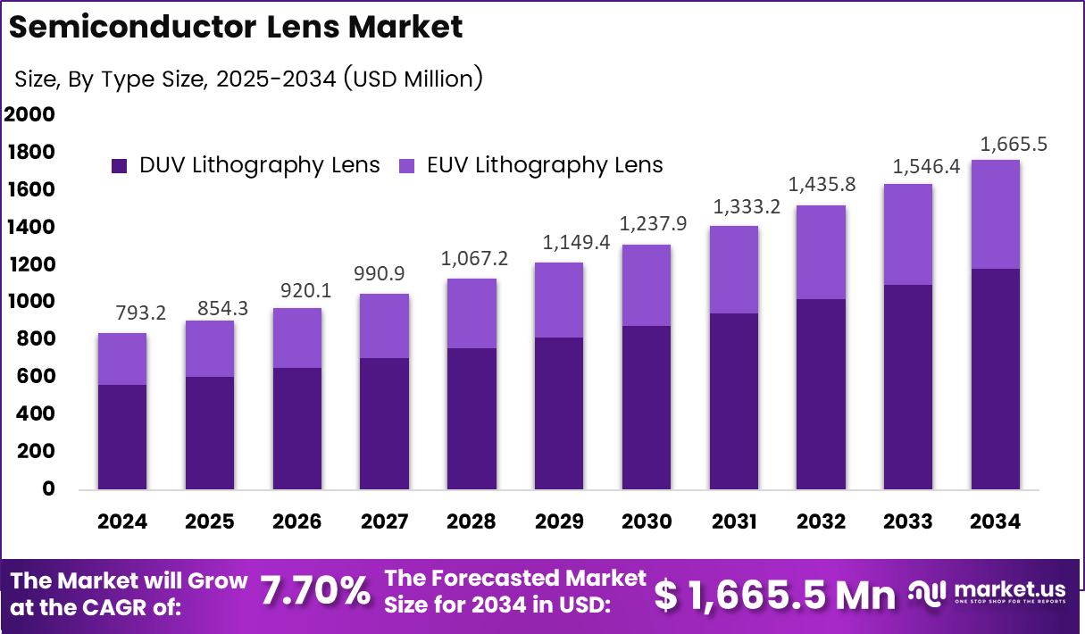
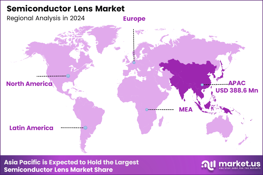
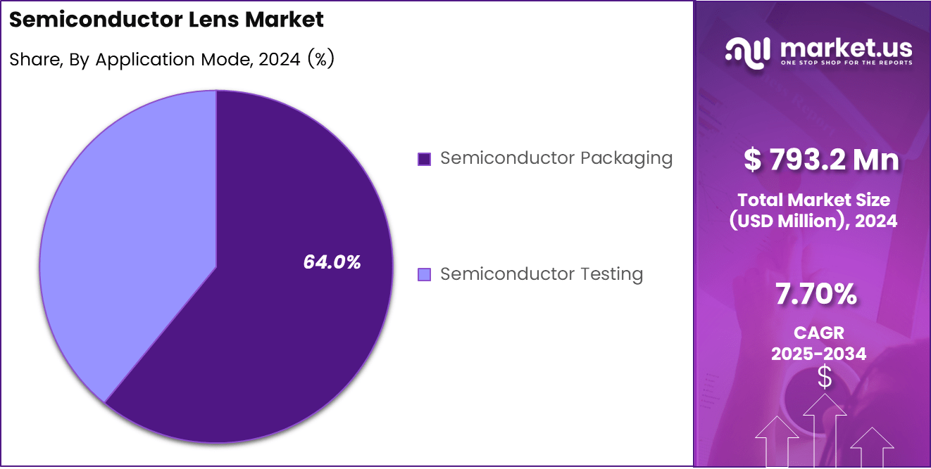
The Global Semiconductor Lens Market generated USD 793.2 Million in 2024 and is predicted to register growth from USD 854.3 Million in 2025 to about USD 1,665.5 Million by 2034, recording a CAGR of 5.94% throughout the forecast span. In 2024, APAC held a dominan market position, capturing more than a 49% share, holding USD 388.6 Million revenue.
The semiconductor lens market refers to the manufacturing and supply of high-precision optical lenses used in semiconductor manufacturing and inspection equipment. These lenses support critical functions such as lithography, metrology, wafer inspection and packaging. As semiconductor manufacturing processes shrink node size and increase complexity, the demand for lenses with tighter tolerances and higher optical performance has grown.
According to Market.us, The Global Semiconductor Market was valued at around USD 840.6 billion in 2024 and is projected to rise from USD 907.4 billion in 2025 to nearly USD 2,010.6 billion by 2034, registering a strong CAGR of 9.2% during the forecast period. This growth is being driven by rising demand for advanced chips used in artificial intelligence, automotive electronics, data centers, and consumer devices.
The core driving factor for the semiconductor lens market is the relentless miniaturization of semiconductor devices. Smaller chip features require lenses with higher resolution and better optical precision. The rapid adoption of technologies such as 5G, artificial intelligence (AI), and high-performance computing intensifies the demand for advanced semiconductor components. This, in turn, increases the need for specialized lenses capable of supporting complex manufacturing processes
Key Takeaways
- DUV (Deep Ultraviolet) lithography lenses dominated with 71%, driven by their essential role in advanced chip patterning and high-precision fabrication.
- Semiconductor packaging applications accounted for 64%, reflecting strong demand for optical precision in wafer-level and microchip assembly processes.
- Asia-Pacific led the global market with 49% share, supported by strong semiconductor manufacturing bases and rapid technology upgrades.
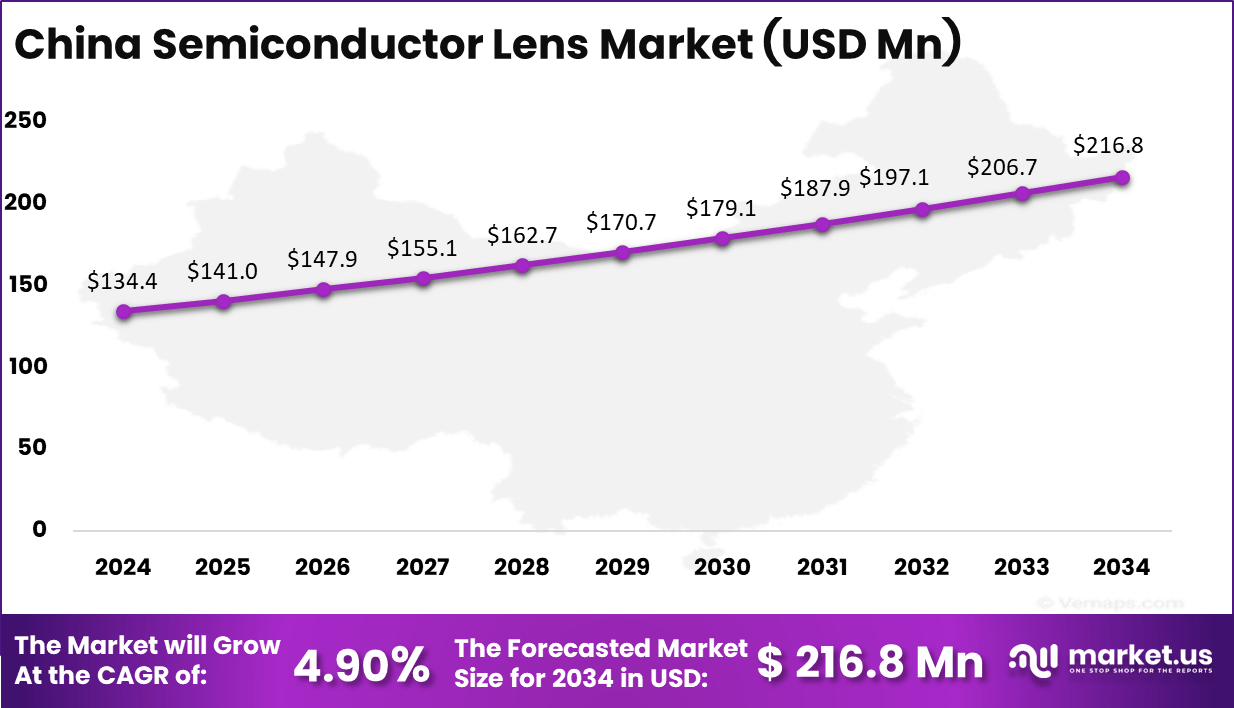
- China reached a valuation of USD 134.4 Million with a moderate 4.9% CAGR, sustained by expanding chip production capacity and local equipment development initiatives.
Analysts’ Viewpoint
Demand for semiconductor lenses correlates strongly with the global semiconductor industry’s growth, which itself clocked a notable growth rate of more than 7% annually in recent years. The demand for lenses is not only in lithography but also in semiconductor testing and packaging, which represents around 10% of the lens market.
The automotive industry alone, requiring advanced chips for driver assistance and infotainment, has increased semiconductor lens demand by approximately 15% over the last two years. Meanwhile, telecommunications, driven by 5G expansion, contributes to about 20% of lens usage related to semiconductor component manufacturing.
EUV lithography technology adoption is rising notably, with EUV lenses increasing their share at a rate of more than 10% CAGR due to their capability to produce extremely small chip features. DUV lenses continue steady growth with 6-7% CAGR, supporting mature semiconductor nodes and processes. Artificial intelligence and machine learning are revolutionizing lens design, optimizing optical performance and reducing manufacturing errors.
Investment and Business Benefits
Investors and manufacturers are channeling funding towards developing novel optical materials, manufacturing precision, and AI-driven design software for lenses. The Asia-Pacific region alone attracts more than 70% of global semiconductor manufacturing investments annually, creating vast opportunities for lens manufacturers.
Furthermore, specialized lenses for burgeoning semiconductor applications like quantum computing and 3D packaging are emerging as profitable niches. Public-sector subsidies and incentives to reduce dependency on foreign semiconductor imports are further catalyzing investment activity in lens innovations.
Businesses involved in high-precision semiconductor lens manufacturing benefit from enhanced technological leadership and entry into growing semiconductor supply chains. Investments in advanced lens technology can lead to significant productivity gains – companies report yield improvements up to 10-12% with better lens quality and inspection systems.
China Market Size
China specifically represents a very significant market within the Asia-Pacific region, with demand for semiconductor lenses reaching approximately 134.4 million units. The country’s rapid expansion of domestic semiconductor manufacturing capacity and strategic initiatives focused on technological independence are primary growth drivers. Investments in advanced lithography and packaging technologies stimulate a sustained need for precise optical components like lenses.
China’s role as an expanding production and innovation center for semiconductor devices places it at the forefront of market growth globally. Continued government incentives and infrastructural development further intensify demand in this critical national market.
The Asia-Pacific region holds a commanding share of 49% in the semiconductor lens market. This dominance is driven by the concentration of major semiconductor manufacturing facilities and fabs across countries such as Taiwan, South Korea, Japan, and increasingly China.
The region is a global hub for semiconductor production and innovation, which fuels the strong demand for advanced optical lenses employed in lithography, testing, and packaging processes. Continued investment in semiconductor infrastructure, government support, and technological advancements contribute to the robust growth in this region.
By Type
In 2024, The DUV lithography lens segment commands a dominant position in the semiconductor lens market, accounting for 71% of the overall share. This strong presence is due to DUV lenses being widely adopted in semiconductor manufacturing processes for mature and advanced nodes. Their ability to enable high-precision patterning using deep ultraviolet light is essential for producing smaller, more complex integrated circuits.
Many established manufacturers focus on refining DUV lens technology to enhance resolution and throughput, supporting steady demand in this segment. Although emerging technologies like EUV lithography gain attention, DUV lenses remain crucial for a significant portion of chip production, especially for applications where cost-efficiency and process maturity matter.
The consistent innovation in material science and optical precision ensures that DUV lenses continue to meet the evolving needs of the semiconductor industry worldwide while balancing performance with manufacturing practicality.
By Application
In 2024, Within the broad range of uses for semiconductor lenses, the packaging segment makes up a notable 64% of the market share. Semiconductor packaging plays a critical role in protecting delicate chips and enhancing their performance by providing mechanical support and thermal management. Reliable and precise lenses are necessary for inspection, testing, and quality control during the packaging stages, ensuring high yields and product reliability.
Advancements in packaging technologies such as 3D integration and wafer-level packaging increase the complexity and demand for sophisticated optical lenses. This segment benefits substantially from ongoing growth in consumer electronics, automotive electronics, and telecommunications, where high-performance and compact chips are continuously required.
Key Market Segment
By Type
- DUV Lithography Lens
- EUV Lithography Lens
By Application
- Semiconductor Testing
- Semiconductor Packaging
Key Regions and Countries
- North America
- US
- Canada
- Europe
- Germany
- France
- The UK
- Spain
- Italy
- Rest of Europe
- Asia Pacific
- China
- Japan
- South Korea
- India
- Australia
- Rest of APAC
- Latin America
- Brazil
- Mexico
- Rest of Latin America
- Middle East & Africa
- GCC
- South Africa
- Rest of MEA
Emerging Trends
- Integration of AI-driven optical correction and real-time defect detection is improving wafer imaging accuracy by nearly 27% in advanced lithography systems.
- Growing adoption of EUV lithography for sub-5 nm and sub-3 nm chip production is boosting demand for ultra-precise semiconductor lenses.
- Development of hybrid refractive–reflective lenses and meta-optics is emerging as a key design trend to enhance light efficiency and reduce system weight.
- Expansion of localized production in Asia-Pacific, supported by national semiconductor initiatives, is strengthening regional self-reliance in lens manufacturing.
- Rising focus on sustainability and energy efficiency is encouraging the use of recyclable optical materials and eco-friendly coating processes.
- Increasing collaboration between optics manufacturers and semiconductor foundries is accelerating innovation in precision lens technology and system integration.
Tpo 5 Use Cases
- Photolithography in Chip Fabrication: Semiconductor lenses are used in DUV and EUV lithography systems to project circuit patterns onto wafers with nanometer-level precision, enabling the production of advanced chips below 5 nm.
- Wafer Inspection and Metrology: High-precision lenses are essential for detecting microscopic defects and ensuring wafer surface uniformity, improving yield rates by nearly 30%.
- Semiconductor Packaging Alignment: Lenses support optical alignment in 3D stacking, flip-chip bonding, and chiplet integration, enhancing packaging accuracy and performance efficiency.
- Optical Testing in Semiconductor Equipment: Used in automated testing systems to validate layer thickness, feature size, and pattern alignment during fabrication and post-processing.
- Research and Development Applications: Advanced lenses are utilized in semiconductor R&D labs for material analysis, photomask inspection, and process simulation, helping achieve higher miniaturization and optical precision for next-generation chip designs.
Driver
Growing Demand for Advanced Semiconductor Devices
The increasing complexity and miniaturization of semiconductor chips are driving strong demand for advanced semiconductor lenses. As industries such as consumer electronics, automotive, and telecommunications push towards smaller, faster, and more efficient chips, lenses used in lithography and testing must keep pace. This ensures higher resolution and precision in manufacturing, which is crucial for technologies like AI, 5G, and IoT.
The need for these highly specialized lenses supports steady market growth with an expanding application base. This driver reflects the semiconductor industry’s broader trend toward enhanced chip performance and density. The introduction of Extreme Ultraviolet (EUV) lithography lenses, which support sub-7nm manufacturing nodes, represents a significant growth frontier, requiring sophisticated optical components.
Restraint
High Manufacturing Costs and Technical Complexity
Producing semiconductor lenses involves advanced materials and intricate manufacturing processes, which leads to very high costs. These lenses must meet stringent quality and precision standards, demanding sophisticated optical designs and cleanroom production environments. The capital intensity of establishing and maintaining such facilities is a significant hurdle for many companies, limiting new entrants and squeezing smaller manufacturers.
Furthermore, the complexity of achieving nanometer-scale accuracy in lenses, especially for EUV lithography, presents technical challenges that require continuous innovation and skilled labor. Shortages in specialized expertise in optics and photonics add to these constraints, slowing down production scale-up and increasing operational costs. This restraint affects the pace of market expansion despite strong product demand.
Opportunity
Adoption of Advanced Packaging and Testing Technologies
The growing focus on semiconductor packaging and testing technologies opens new avenues for semiconductor lens manufacturers. As chips become more complex with multiple layers and integrated functions, testing lenses with enhanced resolution and metrology precision are critical to ensure product quality and yield.
Additionally, next-generation lithography methods and evolving packaging formats, including 3D chip stacking, are expanding the need for innovative lenses. This trend allows companies to capture higher value by catering to niche needs within the broader semiconductor manufacturing ecosystem. Regional specialization and strategic partnerships with foundries and packaging firms further amplify growth prospects for lens makers.
Challenge
Supply Chain Vulnerabilities and Geopolitical Risks
The semiconductor lens market faces significant supply chain risks due to the highly specialized nature of components and materials. Key raw materials and precision manufacturing systems are sourced globally, making the supply chain sensitive to disruptions. Geopolitical tensions, such as trade restrictions and export controls, have intensified uncertainties and constrained the free flow of critical optics technology and parts.
These challenges impact production schedules, cost structures, and market access. Companies must navigate complex international regulations and potential sanctions while ensuring consistent supply to meet rapidly evolving market demands. The need for resilient supply chains and diversified sourcing strategies remains a persistent challenge for semiconductor lens manufacturers aiming for global competitiveness.
SWOT Analysis
Strengths
- High technological precision and optical quality give lens manufacturers a strong competitive edge in semiconductor production.
- Strong demand from advanced chip fabrication for AI, 5G, and automotive applications ensures consistent market stability.
- Established manufacturing bases in the Asia-Pacific provide cost advantages and production scalability.
- Continuous R&D investment improves coating durability, alignment accuracy, and optical resolution.
Weaknesses
- High production and R&D costs limit market accessibility for new entrants.
- Heavy reliance on a few suppliers for specialized optical materials increases supply risk.
- Long development cycles and strict testing slow down product introduction.
- Limited domestic expertise in high-end EUV lens production in emerging economies.
Opportunities
- Adoption of AI-driven lens design and smart optical inspection creates new business models.
- Expanding semiconductor fabrication capacity in China, Japan, and the US fuels demand for precision lenses.
- Rising government funding for semiconductor self-reliance programs supports local lens production.
- Integration of meta-optics and hybrid lens technology opens high-value innovation opportunities.
Threats
- Geopolitical restrictions and trade barriers may affect component availability.
- Rapid technology shifts could make older lens types obsolete within short cycles.
- High competition among global optics giants may pressure margins.
- Market vulnerability to semiconductor industry slowdowns impacts lens demand directly.
Key Player Analysis
The Semiconductor Lens Market is led by global optics and imaging technology leaders such as Carl Zeiss AG, Nikon Corporation, Canon Inc., and ASML Holding NV. These companies play a pivotal role in the lithography and wafer inspection segments by supplying precision optical lenses used in photolithography systems and semiconductor fabrication equipment. manufacturing.
Prominent optical component and material manufacturers such as Hoya Corporation, Corning Incorporated, Jenoptik AG, and Shin-Etsu Chemical Co., Ltd. contribute through the production of specialty glass, quartz, and photo-optical materials. Their expertise supports the development of high-precision lenses with exceptional refractive stability and thermal resistance, catering to semiconductor, laser, and metrology applications.
Emerging and regionally active players including Edmund Optics, Lasertec Corporation, Nanjing Wavelength Opto-Electronic Science & Technology, Shenzhen Canrill Technologies, and Hefei Bohu Optoelectronic Technology, along with other key participants, focus on optical design optimization, coating technology, and inspection optics. Their expanding manufacturing capabilities across Asia-Pacific are strengthening global supply resilience and supporting the growing demand for semiconductor production equipment.
Top Key Player
- Carl Zeiss AG
- Nikon Corporation
- Canon Inc.
- ASML Holding NV
- Hoya Corporation
- Corning Incorporated
- Jenoptik AG
- Shin-Etsu Chemical Co., Ltd.
- Edmund Optics
- Lasertec Corporation
- Nanjing Wavelength Opto-Electronic Science & Technology
- Shenzhen Canrill Technologies
- Hefei Bohu Optoelectronic Technology
- Other Key Players
Recent Development
- September 2025: Carl Zeiss successfully established the new generation AIMS® EUV 3.0 mask qualification tool on the market, which significantly enhances lithography mask inspection capabilities at extreme ultraviolet wavelengths.
- January 2025: Nikon Corporation Launched the Rayfact RF3-6x variable magnification industrial lenses designed for inspecting microscopic patterns on semiconductor wafers, offering improved resolution and defect detection for next-gen semiconductor packaging.
Report Scope
Report Features Description Market Value (2024) USD 793.2 Mn Forecast Revenue (2034) USD 1,665.5 Mn CAGR(2025-2034) 7.70% Base Year for Estimation 2024 Historic Period 2020-2023 Forecast Period 2025-2034 Report Coverage Revenue forecast, AI impact on Market trends, Share Insights, Company ranking, competitive landscape, Recent Developments, Market Dynamics, and Emerging Trends Segments Covered By Type (DUV Lithography Lens, EUV Lithography Lens), By Application (Semiconductor Testing, Semiconductor Packaging) Regional Analysis North America – US, Canada; Europe – Germany, France, The UK, Spain, Italy, Russia, Netherlands, Rest of Europe; Asia Pacific – China, Japan, South Korea, India, New Zealand, Singapore, Thailand, Vietnam, Rest of Latin America; Latin America – Brazil, Mexico, Rest of Latin America; Middle East & Africa – South Africa, Saudi Arabia, UAE, Rest of MEA Competitive Landscape Carl Zeiss AG, Nikon Corporation, Canon Inc., ASML Holding NV, Hoya Corporation, Corning Incorporated, Jenoptik AG, Shin-Etsu Chemical Co., Ltd., Edmund Optics, Lasertec Corporation, Nanjing Wavelength Opto-Electronic Science & Technology, Shenzhen Canrill Technologies, Hefei Bohu Optoelectronic Technology, Other Key Players Customization Scope Customization for segments, region/country-level will be provided. Moreover, additional customization can be done based on the requirements. Purchase Options We have three licenses to choose from: Single User License, Multi-User License (Up to 5 Users), Corporate Use License (Unlimited Users, Printable PDF) 
-
-
Carl Zeiss AG Nikon Corporation Canon Inc. ASML Holding NV Hoya Corporation Corning Incorporated Jenoptik AG Shin-Etsu Chemical Co., Ltd. Edmund Optics Lasertec Corporation Nanjing Wavelength Opto-Electronic Science & Technology Shenzhen Canrill Technologies Hefei Bohu Optoelectronic Technology Other Key Players
Our Clients
- 160866
- Oct 2025