Global Lithography Equipment Market Size, Share, Growth Analysis By Technology (ArF, KrF, i-line, ArF immersion, Extreme Ultraviolet Lithography), By Equipment (Optical Lithography/Photolithography, Mask aligners, Electron beam lithography, Ion lithography, X-Ray lithography, Nanoimprint lithography), By Application (Advanced Packaging, MEMS devices, LED devices, Others), By End Use (Electronics Manufacturing, Healthcare and Life Sciences, Automotive Industry, Telecommunications, Others), By Region and Companies - Industry Segment Outlook, Market Assessment, Competition Scenario, Statistics, Trends and Forecast 2025-2034
- Published date: Sep 2025
- Report ID: 160385
- Number of Pages: 380
- Format:
-
keyboard_arrow_up
Quick Navigation
Report Overview
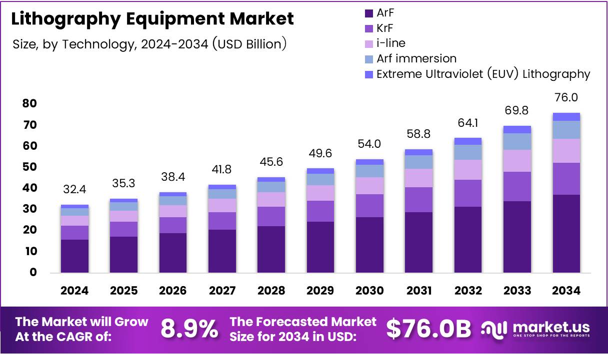
The Global Lithography Equipment Market size is expected to be worth around USD 76.0 Billion by 2034, from USD 31.3 Billion in 2024, growing at a CAGR of 8.9% during the forecast period from 2025 to 2034.
The Lithography Equipment Market represents a critical segment of the semiconductor manufacturing industry, enabling precise pattern transfer onto silicon wafers. It plays a key role in producing integrated circuits and microchips. As demand for advanced electronics grows, lithography tools support innovation in semiconductor fabrication and microelectronic component design globally.
Moreover, the market continues to expand as semiconductor manufacturers invest in EUV (Extreme Ultraviolet) lithography and DUV (Deep Ultraviolet) lithography technologies. These solutions drive smaller node production and higher performance chips. With rising automation and precision requirements, lithography equipment adoption strengthens across consumer electronics, automotive, and industrial applications, fostering substantial capital expenditure.
In addition, growth is propelled by the increasing need for AI-powered chips, 5G infrastructure, and IoT devices. Leading foundries are upgrading facilities, while new players in Asia-Pacific enter the ecosystem. Consequently, demand for advanced patterning technologies intensifies, positioning lithography equipment as a cornerstone in next-generation chip manufacturing.
Furthermore, government investments significantly accelerate the market’s progress. Countries like the U.S., China, Japan, and South Korea are funding semiconductor sovereignty initiatives. Through policy support, subsidies, and tax incentives, they encourage domestic production. Such measures improve local capacity, reduce supply chain dependency, and stimulate long-term lithography equipment procurement.
Regulatory frameworks also shape the competitive environment by promoting intellectual property protection and export control compliance. Stricter environmental standards drive manufacturers to adopt sustainable equipment solutions. Therefore, equipment suppliers focus on energy efficiency, precision optics, and eco-friendly manufacturing processes to align with evolving government mandates and international trade norms.
Additionally, continuous R&D investment from key players like ASML, Nikon, and Canon enhances technological capabilities. These firms prioritize product innovation and collaboration with chipmakers, aiming to achieve finer resolution and higher throughput. As a result, the market sees consistent upgrades in wafer alignment, light source control, and overlay accuracy.
Key Takeaways
- The Global Lithography Equipment Market is projected to reach USD 76.0 Billion by 2034, growing from USD 31.3 Billion in 2024 at a CAGR of 8.9% (2025–2034).
- In 2024, ArF technology led the By Technology segment with a 32.4% share, driven by high resolution and demand for advanced chips.
- Optical Lithography/Photolithography dominated the By Equipment segment in 2024 with a 43.7% share, due to its scalability, precision, and cost-efficiency.
- Advanced Packaging held the top spot in the By Application segment in 2024, accounting for a 39.9% share, fueled by 3D stacking and heterogeneous integration trends.
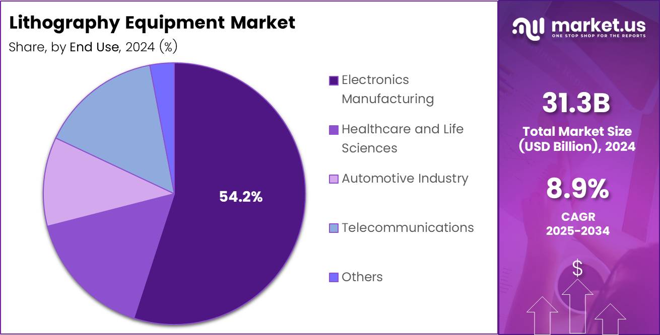
- Electronics Manufacturing was the leading End Use segment in 2024, capturing a 54.2% share, supported by growth in consumer electronics and computing devices.
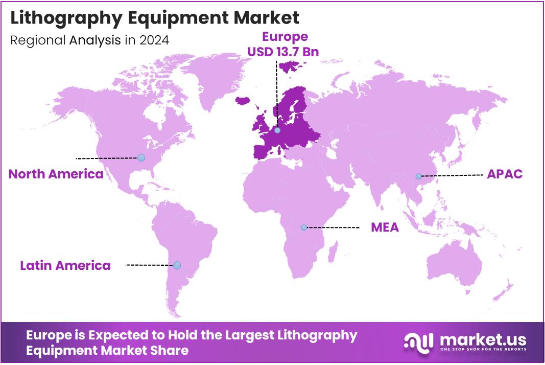
- Europe emerged as the top regional market in 2024, commanding a 43.8% share valued at USD 13.7 Billion, driven by strong semiconductor clusters in the Netherlands, Germany, and France.
By Technology Analysis
ArF dominates with 32.4% due to its precision and widespread adoption in semiconductor manufacturing.
In 2024, ArF held a dominant market position in the By Technology Analysis segment of the Lithography Equipment Market, with a 32.4% share. Its high resolution and capability to produce smaller feature sizes make it a preferred choice for advanced chip fabrication. The increasing demand for microprocessors and memory chips further fuels its growth.
KrF technology continues to play a vital role in semiconductor production. It offers a cost-effective solution for medium-complexity integrated circuits. Many foundries rely on KrF due to its reliability, stability, and compatibility with various substrate materials. This segment remains essential for mid-node semiconductor processes.
i-line lithography remains significant in older-generation semiconductor production and niche applications. It is widely used for MEMS devices and LED manufacturing, thanks to its simplicity and lower operational costs. Despite newer technologies emerging, i-line still serves cost-sensitive and mature process nodes effectively.
ArF immersion technology enables even smaller feature sizes and enhanced pattern resolution. Its ability to increase numerical aperture enhances chip density. Semiconductor manufacturers are increasingly integrating ArF immersion systems to meet advanced node requirements and support innovations in high-performance computing.
Extreme Ultraviolet (EUV) Lithography represents the next frontier in chipmaking. Though costly, it allows patterning at sub-7nm nodes, supporting cutting-edge applications. Major chipmakers invest heavily in EUV to maintain technological leadership. Its adoption is expected to rise as fabrication complexity grows across semiconductor ecosystems.
By Equipment Analysis
Optical Lithography/Photolithography dominates with 43.7% due to its versatility and extensive usage across semiconductor fabs.
In 2024, Optical Lithography/Photolithography held a dominant market position in the By Equipment Analysis segment of the Lithography Equipment Market, with a 43.7% share. This equipment type remains the backbone of semiconductor fabrication, supporting both mature and advanced nodes. Its scalability, precision, and cost-efficiency continue to drive demand globally.
Mask aligners play a critical role in microfabrication processes, particularly for MEMS and micro-optics. These systems offer precise alignment and are valued for their adaptability to diverse wafer sizes. Their cost-effectiveness and simplicity make them ideal for research, prototyping, and low-volume production applications.
Electron beam lithography is renowned for its exceptional resolution, enabling the creation of nanoscale features. It is widely adopted in research labs and for mask writing. Although throughput remains a limitation, its flexibility and direct-write capabilities make it essential for innovation-driven nanotechnology development.
Ion lithography provides high precision and superior depth control. This technology is emerging as a viable solution for next-generation semiconductor structures. Its unique ability to minimize defects and improve pattern fidelity supports its growing relevance in advanced device manufacturing.
X-Ray lithography offers deep penetration and fine feature definition. It is especially suitable for fabricating thick resist layers and high-aspect-ratio structures. Despite limited commercial use, it remains important in specialized microfabrication and research-oriented applications.
Nanoimprint lithography delivers a cost-effective approach for nanoscale patterning. By physically embossing patterns, it reduces complexity and equipment costs. This segment gains traction in applications requiring high resolution and low cost, such as optical devices, displays, and microfluidic components.
By Application Analysis
Advanced Packaging dominates with 39.9% due to rising demand for compact and high-performance semiconductor solutions.
In 2024, Advanced Packaging held a dominant market position in the By Application Analysis segment of the Lithography Equipment Market, with a 39.9% share. Growing emphasis on heterogeneous integration, 3D stacking, and chiplet-based architectures fuels its demand. Lithography tools ensure precision alignment and reliability in packaging innovations.
MEMS devices application continues to expand due to the surge in IoT and sensor-based technologies. Lithography equipment supports micro-scale patterning essential for MEMS fabrication. Increased use in automotive, healthcare, and industrial automation drives its adoption across global markets.
LED devices benefit from lithography’s precision in pattern definition and uniformity. As the LED industry shifts toward micro-LED and mini-LED technologies, lithography tools become critical for achieving fine resolutions. The growing display and lighting sectors further reinforce this segment’s steady growth trajectory.
Others category includes niche applications like photonics, solar cells, and biochips. Each of these sectors leverages lithography for microfabrication accuracy. Continuous research and innovation across emerging technologies expand the scope of lithography usage, fostering diverse application opportunities.
By End Use Analysis
Electronics Manufacturing dominates with 54.2% due to escalating semiconductor demand and ongoing technological advancements.
In 2024, Electronics Manufacturing held a dominant market position in the By End Use Analysis segment of the Lithography Equipment Market, with a 54.2% share. Rapid advancements in consumer electronics, computing devices, and memory technologies drive equipment adoption. Lithography remains vital for producing high-performance, miniaturized electronic components.
Healthcare and Life Sciences sector increasingly adopts lithography for fabricating biochips, diagnostic tools, and lab-on-a-chip systems. The precision offered by lithographic processes enhances device reliability and sensitivity. Expanding applications in genomics, biosensing, and drug discovery further contribute to segmental growth.
Automotive Industry utilizes lithography in manufacturing sensors, power devices, and microcontrollers for smart vehicles. As electric and autonomous vehicles rise, demand for advanced semiconductors intensifies. Lithography ensures production accuracy, supporting innovations in automotive safety and efficiency.
Telecommunications relies on lithography for high-speed chips and optical components. The rollout of 5G and forthcoming 6G networks boosts equipment requirements. Precise lithographic techniques enable compact, energy-efficient designs, critical for evolving communication infrastructure.
Others segment encompasses industries such as aerospace, defense, and energy. These sectors demand specialized microfabrication solutions for advanced systems. Lithography tools help create complex structures and enhance device performance, sustaining steady adoption across these niche markets.
Key Market Segments
By Technology
- ArF
- KrF
- i-line
- ArF immersion
- Extreme Ultraviolet (EUV) Lithography
By Equipment
- Optical Lithography/Photolithography
- Mask aligners
- Electron beam lithography
- Ion lithography
- X-Ray lithography
- Nanoimprint lithography
By Application
- Advanced Packaging
- MEMS devices
- LED devices
- Others
By End Use
- Electronics Manufacturing
- Healthcare and Life Sciences
- Automotive Industry
- Telecommunications
- Others
Drivers
Rising Demand for Advanced Semiconductor Nodes in Chip Fabrication Drives Market Growth
The Lithography Equipment Market is witnessing robust growth as chip manufacturers increasingly demand advanced semiconductor nodes below 7nm. This shift is driven by the growing need for high-performance computing and energy-efficient devices. As transistor density rises, lithography tools capable of extreme precision, like EUV systems, become vital for next-generation fabrication.
Furthermore, escalating investments in AI, IoT, and 5G infrastructure are fueling the adoption of leading-edge chips. These technologies require high-speed processing, low latency, and miniaturized circuits, all of which rely on advanced lithographic precision. Governments and private sectors are boosting semiconductor R&D, accelerating equipment deployment across fabrication facilities worldwide.
Additionally, the expansion of foundry capacities in regions like East Asia and the U.S. strengthens market dynamics. Countries such as Taiwan, South Korea, and the U.S. are incentivizing local semiconductor production to reduce supply chain dependency. These developments enhance demand for EUV and DUV systems to support mass production of high-end chips.
Lastly, continuous innovation in EUV and DUV lithography enhances throughput, overlay accuracy, and cost efficiency. Equipment makers are integrating AI-based alignment and optical improvements to optimize wafer patterning. Such technological progress not only boosts production yield but also reinforces market competitiveness amid rapid semiconductor evolution.
Restraints
Supply Chain Vulnerabilities in Critical Components and Optics Restrains Market Growth
The Lithography Equipment Market faces challenges due to supply chain vulnerabilities in critical components like lasers, mirrors, and optics. These parts, often sourced from specialized suppliers, have limited global availability, creating production bottlenecks and extending lead times for manufacturers.
Moreover, complex maintenance and calibration requirements add operational constraints. Lithography systems, particularly EUV machines, demand continuous precision tuning and contamination control. This leads to longer downtimes and higher servicing costs, affecting productivity for semiconductor fabs operating on tight production schedules.
In addition, the market struggles with a limited skilled workforce trained in EUV system operation. Managing sophisticated optics and vacuum environments requires deep technical knowledge, which remains scarce globally. The shortage of qualified engineers and technicians hampers smooth system installation, calibration, and optimization across new and expanding fabs.
As semiconductor processes scale toward sub-2nm nodes, these operational barriers become more pronounced. Equipment makers and fabs must invest in training programs, localized component sourcing, and supply chain diversification to reduce risks and sustain production continuity in an increasingly technology-intensive landscape.
Growth Factors
Integration of AI-Based Process Control in Lithography Systems Creates Growth Opportunities
The integration of AI-based process control represents a transformative growth opportunity in the Lithography Equipment Market. By using machine learning algorithms, fabs can achieve real-time defect detection, pattern optimization, and process stabilization, leading to improved wafer yields and reduced variability.
Additionally, the rising adoption of 3D NAND and DRAM manufacturing technologies opens new avenues. These memory architectures require multi-layer patterning and high-aspect-ratio etching, demanding advanced DUV and EUV tools for precise feature alignment. This trend enhances lithography demand in both logic and memory production segments.
The emergence of advanced packaging and heterogeneous integration further expands opportunities. As chipmakers move beyond traditional scaling, they focus on chiplet integration, 2.5D/3D stacking, and fan-out wafer-level packaging, all reliant on high-accuracy lithography for interconnect patterning.
Collectively, these innovations strengthen the role of lithography as a key enabler of next-generation semiconductor manufacturing. Companies investing in AI-driven control systems and versatile lithography tools are well-positioned to capture market share and support evolving fabrication requirements across global foundries.
Emerging Trends
Transition Toward High-NA EUV Lithography for Sub-2nm Nodes Defines Market Trends
A major trend shaping the Lithography Equipment Market is the transition toward High-NA EUV lithography to support sub-2nm node development. This breakthrough technology improves resolution, enhances depth of focus, and enables patterning of ultra-fine features essential for future chip scaling.
Additionally, strategic partnerships between equipment vendors and foundries are increasing. Collaborations help accelerate technology validation, pilot production, and cost-sharing for complex tool development. Such alliances foster innovation ecosystems vital for EUV and DUV ecosystem maturity.
There’s also a growing focus on sustainability and energy-efficient fabrication. Lithography systems are energy-intensive, prompting vendors to adopt green manufacturing and resource-efficient cooling solutions. Sustainable practices help fabs meet environmental regulations and reduce carbon footprints across semiconductor production lines.
Finally, the development of compact lithography tools tailored for R&D and prototyping is gaining traction. Smaller, cost-effective systems empower research institutes and startups to test novel materials and device architectures, nurturing innovation pipelines that ultimately enhance market depth and technology adoption.
Regional Analysis
Europe Dominates the Lithography Equipment Market with a Market Share of 43.8%, Valued at USD 13.7 Billion
In 2024, Europe emerged as the leading region in the global lithography equipment market, holding a 43.8% share, valued at approximately USD 13.7 Billion. The region’s dominance is driven by robust semiconductor manufacturing clusters in the Netherlands, Germany, and France.
Strong government backing for chip sovereignty and technological innovation in EUV and DUV systems enhances its leadership position. Europe’s focus on sustainable chip production and advanced R&D infrastructure continues to attract substantial foreign investments, supporting long-term market stability.
North America Lithography Equipment Market Trends
North America follows closely, supported by significant investments in semiconductor fabrication by the U.S. and Canada. The CHIPS and Science Act has accelerated regional foundry expansion, particularly for advanced logic and memory nodes. Rising adoption of AI, data centers, and 5G technologies fuels demand for precision lithography systems. The region’s ecosystem of R&D centers and partnerships with global equipment suppliers ensures continuous technological upgrades.
Asia Pacific Lithography Equipment Market Trends
Asia Pacific remains a critical hub, with nations like Japan, South Korea, Taiwan, and China driving large-scale chip fabrication. Government incentives and capacity expansion by leading foundries contribute to high equipment demand. Rapid urbanization, digitalization, and rising consumer electronics production further strengthen the region’s market outlook. Continuous technological innovation supports sustained growth.
Middle East and Africa Lithography Equipment Market Trends
In the Middle East and Africa, the lithography equipment market is still emerging, with growth supported by digital infrastructure development and industrial diversification efforts. Countries like the UAE and Saudi Arabia are investing in semiconductor R&D and manufacturing as part of broader tech transformation strategies. Regional adoption is expected to increase as local ecosystems mature.
Latin America Lithography Equipment Market Trends
Latin America’s lithography equipment market is gradually expanding, led by Brazil and Mexico. Growth stems from rising interest in electronics manufacturing and partnerships with global semiconductor players. Although currently limited in scale, ongoing investments in industrial automation and research capabilities are anticipated to create new opportunities for lithography equipment suppliers over the forecast period.
Key Regions and Countries
North America
- US
- Canada
Europe
- Germany
- France
- The UK
- Spain
- Italy
- Rest of Europe
Asia Pacific
- China
- Japan
- South Korea
- India
- Australia
- Rest of APAC
Latin America
- Brazil
- Mexico
- Rest of Latin America
Middle East & Africa
- GCC
- South Africa
- Rest of MEA
Key Lithography Equipment Company Insights
In 2024, the global Lithography Equipment Market showcased strong leadership by ASML Holding NV, which continued to dominate due to its cutting-edge EUV (Extreme Ultraviolet) systems. The company’s focus on high-resolution and miniaturization technologies strengthened its position among advanced semiconductor manufacturers. Its strategic investments in R&D supported next-generation chip fabrication processes.
Nikon Corporation maintained a solid foothold through its deep ultraviolet (DUV) lithography solutions, widely adopted in memory and logic chip production. The firm’s continuous innovation in immersion and ArF scanners enhanced productivity, meeting rising demands from foundries expanding capacity in Asia and the U.S. Nikon’s balanced portfolio catered to both leading-edge and mature node markets.
Canon, Inc. remained a competitive player with its strong emphasis on i-line and KrF lithography tools designed for specialty and display applications. The company focused on cost-efficient solutions for mid-range semiconductor fabrication, leveraging its optics expertise. Canon’s progress in nanoimprint lithography technology also indicated its push toward emerging fabrication alternatives.
EV Group strengthened its presence by offering advanced wafer bonding and nanoimprint lithography systems, crucial for MEMS, photonics, and heterogeneous integration. The company’s expansion in 3D integration and wafer-level packaging aligned with the market’s move toward compact, high-performance devices. Its collaborations with research institutes fostered adoption of emerging semiconductor processes.
Top Key Players in the Market
- ASML Holding NV
- Nikon Corporation
- Canon, Inc.
- EV Group
- Veeco Instruments Inc.
- SUSS MicroTec SE
- Shanghai Micro Electronics Equipment (Group) Co. Ltd.
- Neutronix Quintel Inc.
- JEOL Ltd.
- Onto Innovation
Recent Developments
- In Jul 2025, Multibeam secured USD 31 million in Series B financing to accelerate the global deployment of its E-Beam lithography production solutions. This funding will enhance manufacturing scalability, expand R&D capabilities, and strengthen its position in advanced semiconductor fabrication.
- In Sep 2025, ASML announced plans to take a major stake in Mistral AI with a USD 1.5 billion investment. The move aims to integrate AI-driven modeling into chip design workflows, boosting lithography precision and reinforcing ASML’s strategic foothold in semiconductor innovation.
- In Sep 2024, ZEISS SMT agreed to acquire a Swiss high-tech company, expanding its competencies in precision optics and semiconductor metrology. The acquisition supports ZEISS’s ambition to advance lithography component technology and strengthen its European innovation network.
- In Mar 2025, Silvaco expanded its product portfolio through the acquisition of Cadence’s Process Proximity Compensation Product Line. This strategic move enhances Silvaco’s process simulation offerings, enabling improved accuracy in semiconductor design and bridging gaps in advanced node development.
Report Scope
Report Features Description Market Value (2024) USD 31.3 Billion Forecast Revenue (2034) USD 76.0 Billion CAGR (2025-2034) 8.9% Base Year for Estimation 2024 Historic Period 2020-2023 Forecast Period 2025-2034 Report Coverage Revenue Forecast, Market Dynamics, Competitive Landscape, Recent Developments Segments Covered By Technology (ArF, KrF, i-line, ArF immersion, Extreme Ultraviolet Lithography), By Equipment (Optical Lithography/Photolithography, Mask aligners, Electron beam lithography, Ion lithography, X-Ray lithography, Nanoimprint lithography), By Application (Advanced Packaging, MEMS devices, LED devices, Others), By End Use (Electronics Manufacturing, Healthcare and Life Sciences, Automotive Industry, Telecommunications, Others) Regional Analysis North America (US and Canada), Europe (Germany, France, The UK, Spain, Italy, and Rest of Europe), Asia Pacific (China, Japan, South Korea, India, Australia, and Rest of APAC), Latin America (Brazil, Mexico, and Rest of Latin America), Middle East & Africa (GCC, South Africa, and Rest of MEA) Competitive Landscape ASML Holding NV, Nikon Corporation, Canon, Inc., EV Group, Veeco Instruments Inc., SUSS MicroTec SE, Shanghai Micro Electronics Equipment (Group) Co. Ltd., Neutronix Quintel Inc., JEOL Ltd., Onto Innovation Customization Scope Customization for segments, region/country-level will be provided. Moreover, additional customization can be done based on the requirements. Purchase Options We have three licenses to opt for: Single User License, Multi-User License (Up to 5 Users), Corporate Use License (Unlimited User and Printable PDF)  Lithography Equipment MarketPublished date: Sep 2025add_shopping_cartBuy Now get_appDownload Sample
 -
-
- ASML Holding NV
- Nikon Corporation
- Canon, Inc.
- EV Group
- Veeco Instruments Inc.
- SUSS MicroTec SE
- Shanghai Micro Electronics Equipment (Group) Co. Ltd.
- Neutronix Quintel Inc.
- JEOL Ltd.
- Onto Innovation
Our Clients
- 160385
- Sep 2025