Global Electron Microscope for Semiconductor Market Size, Share, Industry Analysis Report By Type (Scanning Electron Microscopy (SEM), Transmission Electron Microscopy (TEM), Focused Ion Beam (FIB) Systems, Others), By Application (Wafer Inspection & Defect Analysis, Process Development & R&D, Failure Analysis, Quantum Technology & Advanced Devices, Others), By End User (Industries, Academic and Research Institutes, Others), By Regional Analysis, Global Trends and Opportunity, Future Outlook By 2025-2034
- Published date: Oct. 2025
- Report ID: 161149
- Number of Pages: 237
- Format:
-
keyboard_arrow_up
Quick Navigation
Report Overview
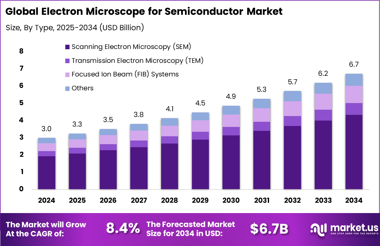
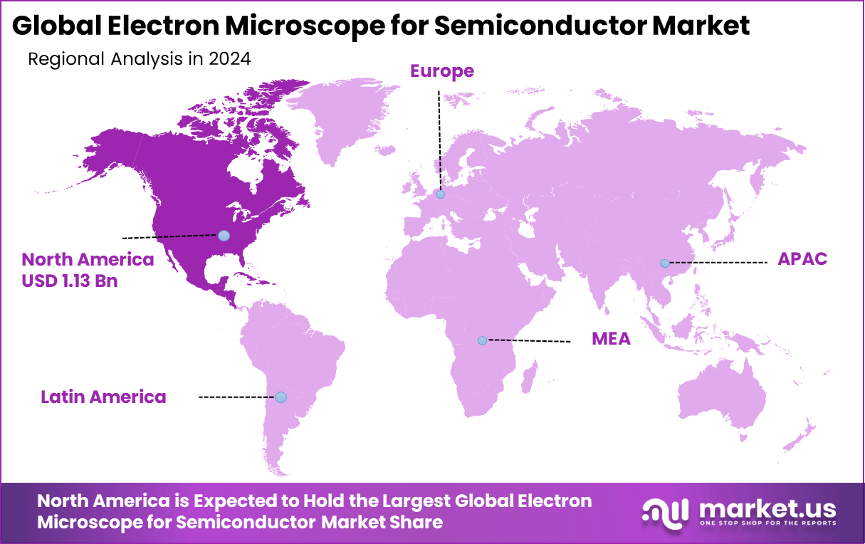
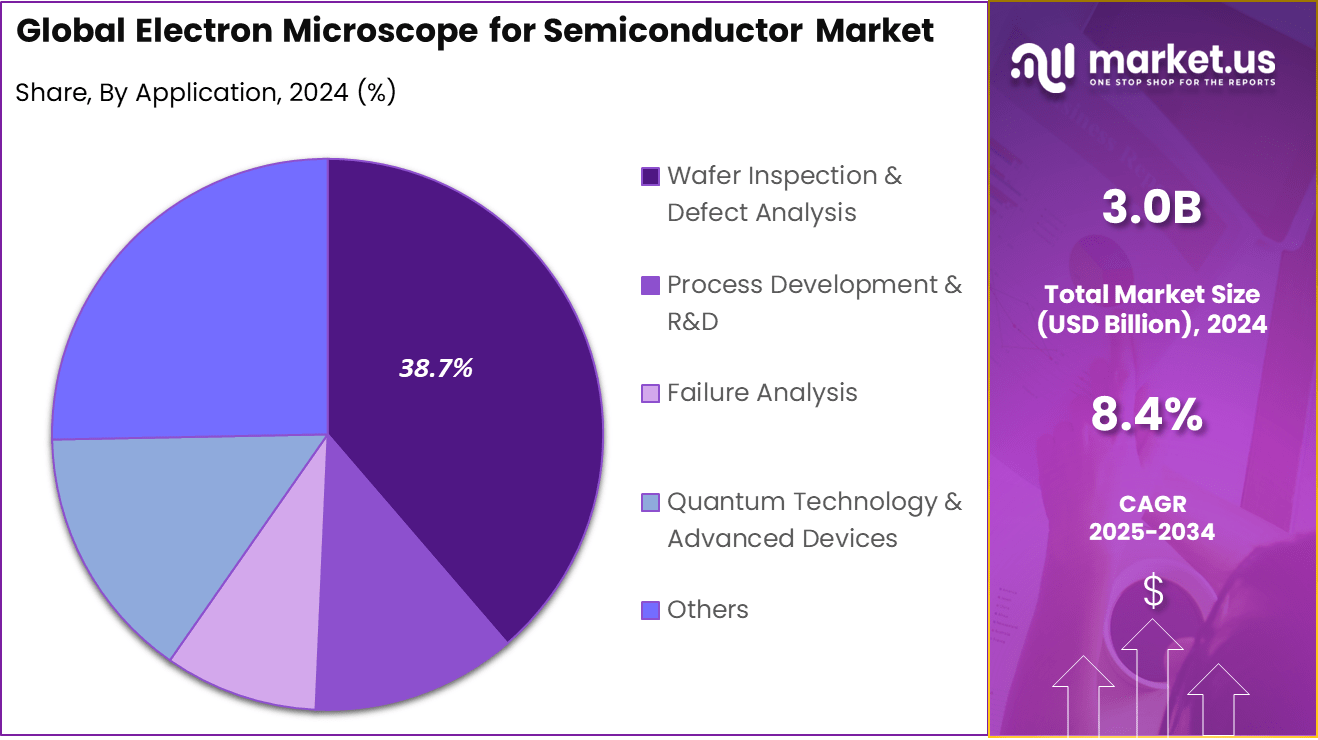
The Global Electron Microscope for Semiconductor Market size is expected to be worth around USD 6.7 billion by 2034, from USD 3.0 billion in 2024, growing at a CAGR of 8.4% during the forecast period from 2025 to 2034. In 2024, North America held a dominant market position, capturing more than a 37.8% share, holding USD 1.13 billion in revenue.
The Electron Microscope for Semiconductor Market is an essential segment within the semiconductor industry that focuses on using advanced electron microscopy tools to analyze and inspect semiconductor materials and devices at the nanoscale. These microscopes provide incredibly high-resolution imaging, which is vital for managing the complexity of modern semiconductor manufacturing, including quality control, defect detection, failure analysis, and research.
As semiconductor devices continue to shrink and designs become more intricate, electron microscopes serve as critical instruments to maintain the high standards necessary for performance and reliability. Top driving factors for this market include the relentless push towards smaller and more efficient electronic chips, driven by consumer electronics, automotive systems, telecommunications, and emerging technologies like artificial intelligence and 5G.
For instance, in September 2025, researchers at Lawrence Berkeley National Laboratory used a cutting-edge 4D Scanning Transmission Electron Microscopy (4D-STEM) technique, enhanced with energy filtering and machine learning, to visualize short-range atomic order (SRO) in semiconductor materials. This breakthrough revealed that even trace elements like tin and silicon arrange themselves in distinct local patterns, significantly influencing electronic properties like the band gap.
Quick Market Facts
- By type, Scanning Electron Microscopy (SEM) dominates with 64.7%, driven by its precision in high-resolution imaging for semiconductor structures.
- By application, wafer inspection and defect analysis accounts for 38.7%, reflecting its critical role in ensuring chip quality and yield.
- By end user, industries lead with 48.5%, showcasing strong adoption for large-scale semiconductor fabrication and R&D.
- North America contributes 37.8%, supported by advanced semiconductor manufacturing and research infrastructure.
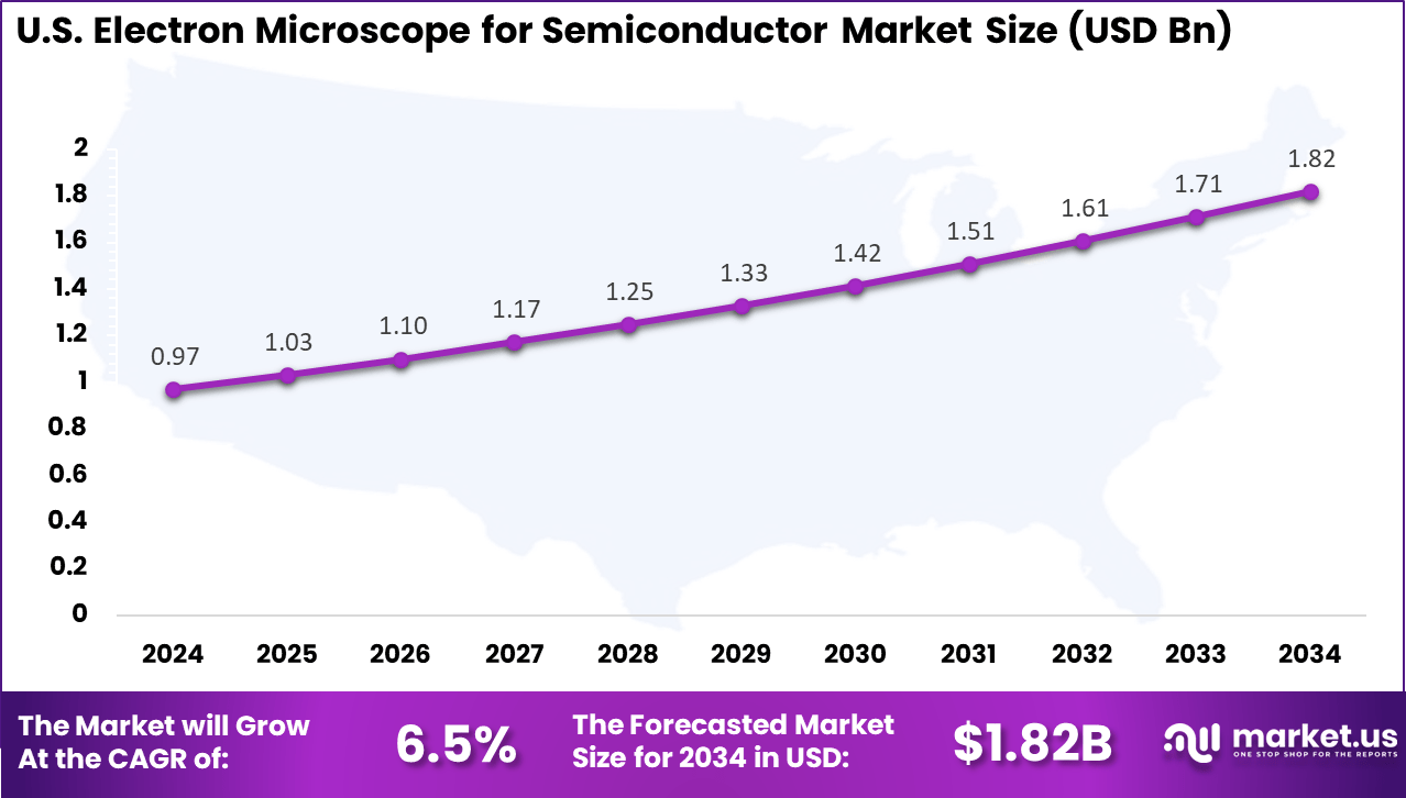
- The US market reached USD 0.97 billion and is growing at a steady CAGR of 6.5%, highlighting its leadership in advanced microscopy adoption for semiconductor production.
Role of Generative AI
Generative AI is redefining semiconductor manufacturing by accelerating chip design and process optimization. AI algorithms analyze vast data from electron microscopes to detect defects faster and more accurately, reducing production errors and boosting yields. In 2023, approximately 72% of semiconductor professionals believed generative AI’s impact would be high to transformative.
This AI-driven approach not only speeds up creating new semiconductor designs but also enhances manufacturing processes by predicting potential faults before they occur, thus increasing efficiency. With semiconductor firms investing hundreds of millions in AI tools, generative AI is becoming a foundational element in chip innovation, allowing for the development of higher-quality chips at a faster pace and with lower costs
U.S. Market Size
The market for Electron Microscope for Semiconductor within the U.S. is growing tremendously and is currently valued at USD 0.97 billion, the market has a projected CAGR of 6.5%. The market is growing rapidly due to significant federal investments under the CHIPS and Science Act, which aim to strengthen domestic semiconductor manufacturing.
As companies expand advanced fabrication facilities, there is increased demand for high-resolution inspection and metrology tools to support cutting-edge process nodes. Additionally, the U.S. leads in semiconductor R&D and innovation, driving the need for electron microscopy in material analysis, defect detection, and process optimization.
For instance, in January 2025, UCLA became one of the first U.S. universities to install the Thermo Fisher Scientific Krios G4 cryo-electron microscope, marking a significant milestone in North America’s leadership in advanced electron microscopy. The system delivers nearly double the resolution and nine times faster data acquisition than previous models, supporting atomic-level imaging for research and semiconductor-related applications.
In 2024, North America held a dominant market position in the Global Electron Microscope for Semiconductor Market, capturing more than a 37.8% share, holding USD 1.13 billion in revenue. The dominance is due to strong government funding, technological leadership, and the presence of major semiconductor manufacturers.
Initiatives like the CHIPS and Science Act spurred significant investment in domestic chip production, driving demand for advanced inspection and metrology tools. Additionally, the region’s strong presence of leading semiconductor companies, advanced research institutions, and technological innovation ecosystems has reinforced North America’s leadership in adopting cutting-edge electron microscopy solutions for quality control and process optimization.
Investment and Business Benefits
Investment opportunities abound as semiconductor manufacturing expands globally, especially with reshoring efforts in regions like the United States, supported by legislation encouraging domestic chip production and equipment manufacturing. Funding for innovation in inspection equipment creates fertile ground for companies developing electron microscopy tools enhanced with AI capabilities.
Smaller benchtop and more affordable models also open up opportunities in educational and smaller R&D settings, broadening the customer base. The business benefits of using electron microscopes in semiconductor production are substantial. They improve yield through early defect detection and failure analysis, reducing costly production errors.
Electron microscopes enable the development of cutting-edge semiconductor materials and devices, thus maintaining competitive advantage in technology-critical sectors. They also streamline quality assurance processes, leading to higher efficiency and reliability in manufacturing.
Type Analysis
In 2024, The Scanning Electron Microscopy (SEM) segment held a dominant market position, capturing a 64.7% share of the Global Electron Microscope for Semiconductor Market. The dominance is driven by its versatility, cost-effectiveness, and simplified sample preparation. SEM is particularly well-suited for high-resolution surface imaging and defect detection, making it essential for routine process monitoring, failure analysis, and quality control in fabs.
Its capability to provide detailed morphological and compositional data enhances its value in semiconductor workflows. Additionally, ongoing technological advancements, increased R&D efforts, and growing demand for nanoscale precision continue to fuel the adoption of SEM systems.
For Instance, in April 2025, NIST launched a study aimed at enhancing the effectiveness of scanning electron microscopy (SEM) in semiconductor applications. Funded under the CHIPS Metrology Program, the initiative focuses on improving how SEM images are interpreted by refining models of electron scattering, particularly for low-energy secondary electrons critical to surface analysis.
Application Analysis
In 2024, the Wafer Inspection & Defect Analysis segment held a dominant market position, capturing a 38.7% share of the Global Electron Microscope for Semiconductor Market. This dominance is due to the crucial role wafer inspection and defect analysis play in ensuring high-yield, fault-free semiconductor production.
These systems are crucial for identifying defects early in the fabrication process, reducing failures, and enhancing product reliability. The increasing demand for advanced semiconductors in applications such as AI, 5G, and autonomous vehicles is accelerating the need for high-precision inspection tools, including electron beam technologies. This trend continues to strengthen the market presence.
For instance, in June 2025, researchers introduced a novel AI-based method for wafer defect classification using scanning electron microscope (SEM) images. Presented at the SEMI Advanced Semiconductor Manufacturing Conference, the study applied Vision Transformers (ViT) to analyze over 7,400 SEM images from 300mm wafers, classifying 11 defect types with over 90% accuracy using as few as 15 samples per class.
End User Analysis
In 2024, The Industries segment held a dominant market position, capturing a 48.5% share of the Global Electron Microscope for Semiconductor Market. This dominance is due to semiconductor and electronics manufacturers’ heavy reliance on EM for process control, failure analysis, quality assurance, and yield management.
Industrial fabs require real‑time, high‑precision imaging to detect defects and optimize production. In addition, growing R&D investments, expansion of fabrication capacity, and demand for nanotechnology solutions across industrial users bolster this market.
For Instance, In October 2024, ZEISS opened a Semiconductor Applications Laboratory in Dresden to support industrial users with advanced microscopy. The facility focuses on physical failure analysis, materials research, and yield improvement using Crossbeam FIB-SEM technology. Located in a key semiconductor hub, it enables close collaboration with chipmakers and uses automated workflows to speed up root-cause analysis.
Emerging Trends
A significant emerging trend in the electron microscope market for semiconductors is the integration of automation and advanced AI-powered analysis. Automated electron microscopes now feature enhanced sample handling and image acquisition, enabling higher throughput and precision in defect identification. This capability is essential as semiconductor manufacturing demands rapid inspection of millions of chips with nanoscale accuracy.
Furthermore, the merging of big data analytics with electron microscopy information allows quicker interpretation of complex imaging, which supports faster decision-making in production environments. Another rising trend is the development of electron microscopes with improved resolution capabilities to keep pace with the miniaturization of semiconductor components.
Instruments are continuously being refined to provide atomic-level imaging, essential for evaluating next-generation semiconductors using new materials like silicon carbide and gallium nitride. This advancement further helps researchers and manufacturers understand material behavior at the smallest scales, which is critical for producing more energy-efficient and powerful semiconductor devices.
Growth Factors
The growth of the electron microscope segment in semiconductors is primarily driven by the continual shrinking of semiconductor devices, requiring high-resolution imaging to identify defects and assure quality at nanoscale levels. Increasing demand for advanced chips in sectors like 5G, artificial intelligence, and Internet of Things (IoT) further fuels this need.
Each new chip generation requires more precise inspection, making electron microscopy essential for semiconductor quality control and failure analysis. Another considerable driver is the growing adoption of novel semiconductor materials such as silicon carbide and gallium nitride.
These materials offer superior performance for applications in electric vehicles and power electronics but require detailed characterization techniques to optimize manufacturing. Electron microscopes provide this essential feedback, facilitating the transition to these next-generation semiconductor technologies and supporting wider industrial adoption.
Key Market Segments
By Type
- Scanning Electron Microscopy (SEM)
- Transmission Electron Microscopy (TEM)
- Focused Ion Beam (FIB) Systems
- Others
By Application
- Wafer Inspection & Defect Analysis
- Process Development & R&D
- Failure Analysis
- Quantum Technology & Advanced Devices
- Others
By End User
- Industries
- Academic and Research Institutes
- Others
By Region
- North America
- Europe
- Asia Pacific
- Latin America
- Middle East & Africa
Drivers
Rising Demand for Precise Semiconductor Analysis
The growth of electron microscopes in the semiconductor industry is largely driven by the increasing need for high-accuracy imaging and defect detection. As semiconductor devices become smaller and more complex, manufacturers rely heavily on electron microscopy to ensure quality and performance. These microscopes enable detailed examination of nanostructures and material defects that are impossible to see with traditional tools.
The rise in technological innovations such as 5G, artificial intelligence, and IoT is also creating a higher demand for smaller, more powerful chips. Electron microscopes are critical in this context because they provide the resolution necessary for manufacturing these advanced components. Governments and industry players are investing heavily in research and development, which boosts the adoption of electron microscopy for ongoing material innovation.
For instance, In October 2025, India launched a $1.2 trillion Bharat 6G Mission to strengthen its position in next-generation connectivity. A key pillar of this effort is the India Semiconductor Mission (ISM), backed by $9 billion to boost domestic chip design and manufacturing. By linking 6G R&D with semiconductor innovation, the plan aims to cut dependence on foreign tech and establish India as a global semiconductor hub.
Restraint
High Cost and Limited Accessibility
One of the main restraints hindering the widespread use of electron microscopes is their high cost. These instruments are expensive to purchase, often running into millions of dollars, which makes them unaffordable for smaller labs and emerging markets. Additionally, their maintenance and operational expenses are substantial, requiring specialized trained staff to operate them effectively.
Furthermore, electron microscopes are complex tools that demand extensive training and expertise, restricting access to a smaller pool of skilled operators. The need for controlled environments such as high vacuum conditions increases operational challenges and discourages many potential users.
For instance, In January 2025, CIQTEK outlined the major cost challenges associated with scanning electron microscopy (SEM). It noted that maintenance, vacuum pump servicing, electron source replacements, calibration, and service contracts significantly increase expenses. The report also stressed that long-term ownership costs often surpass the initial purchase, particularly in high-volume semiconductor settings.
Opportunities
Technological Innovation for Cost Reduction
Technological advancements present significant opportunities to democratize electron microscope access and expand market reach. Innovations aimed at miniaturizing and simplifying these devices could make them more affordable and portable. For example, the development of compact electron microscopes allows smaller research institutions and industries to perform high-resolution inspections without needing large, costly setups.
Another promising opportunity lies in integrating artificial intelligence and automation into electron microscopy. Such innovations can enhance image processing, reduce the need for highly skilled operators, and improve the speed and accuracy of analysis. Implementing these improvements could lower operational costs and enable real-time defect detection in manufacturing lines.
For instance, in April 2025, NIST launched a multi-year study to advance the precision of scanning electron microscopy (SEM) in semiconductor manufacturing. Funded by the CHIPS Metrology Program, the initiative focuses on improving the interpretation of SEM images by refining models of electron scattering, especially for low-energy secondary electrons that are critical for surface imaging.
Challenges
Technical and Operational Limitations
A key challenge of electron microscopy remains the technical complexity and operational limitations. These instruments require a controlled environment with vibrations and electromagnetic interference tightly minimized to produce reliable images. Biological specimens are particularly difficult to analyze because they are sensitive to radiation, vacuum conditions, and sample preparation processes, which can damage or alter their structure.
Moreover, current systems often face limitations in speed, restrictively balancing between area coverage and resolution. Additionally, there are specific challenges related to the analysis of biological and microbial samples, which need special handling to prevent dehydration or radiation damage. Overcoming these issues requires ongoing innovation and investment in faster, more versatile systems that can handle a wider range of samples reliably. This technical challenge remains a concern for further advancing the utility of electron microscopes.
For instance, in August 2024, researchers at the Paul Scherrer Institute set a new benchmark in semiconductor imaging by achieving 4-nanometer resolution using non-destructive X-ray ptychography. This breakthrough underscores growing competition from alternative inspection technologies, as X-ray imaging now offers deep, internal visualization of chips without physical sectioning.
Key Players Analysis
The Electron Microscope for Semiconductor Market is led by major instrumentation providers such as Thermo Fisher Scientific Inc., JEOL Ltd., and ZEISS Group. These companies supply high-resolution electron microscopes that support wafer inspection, defect analysis, and materials characterization. Their systems are widely used in semiconductor fabrication, research labs, and quality assurance processes to ensure nanoscale precision and manufacturing efficiency.
Notable contributors such as Hitachi High-Tech India Private Limited, Leica Microsystems, and Nanoscience Instruments offer advanced scanning electron microscopes (SEM), transmission electron microscopes (TEM), and focused ion beam (FIB) tools. Their equipment enables failure analysis, layer imaging, and process validation in chip design and packaging applications, helping semiconductor manufacturers meet strict performance standards.
Emerging and region-specific players including Orbit & Skyline, Inc., Inquivix Technologies Inc., and other key participants provide complementary technologies, maintenance services, and tailored solutions for semiconductor inspection workflows. Their presence strengthens accessibility, customization, and after-sales support, contributing to broader adoption across global fabrication and R&D facilities.
Top Key Players in the Market
- Thermo Fisher Scientific Inc.
- Hitachi High-Tech India Private Limited
- Orbit & Skyline, Inc.
- JEOL Ltd.
- Nanoscience Instruments
- Leica Microsystems
- ZEISS Group
- Inquivix Technologies Inc.
- Others
Recent Developments
- In March 2025, Thermo Fisher Scientific announced the launch of its Vulcan™ Automated Lab system, designed to integrate electron microscopy and complementary analysis tools into a unified, automated platform. This innovation is aimed at boosting productivity, improving yield, and lowering operational costs for semiconductor manufacturers.
- In June 2023, Thermo Fisher Scientific launched the Metrios 6 Scanning Transmission Electron Microscope (S)TEM, a next-generation, fully automated metrology solution for semiconductor manufacturing. Designed to boost productivity by up to 20%, it leverages advanced machine learning, new hardware, and fast compositional analysis to deliver high-volume, high-quality data.
Report Scope
Report Features Description Market Value (2024) USD 3.0 Bn Forecast Revenue (2034) USD 6.7 Bn CAGR(2025-2034) 8.4% Base Year for Estimation 2024 Historic Period 2020-2023 Forecast Period 2025-2034 Report Coverage Revenue forecast, AI impact on Market trends, Share Insights, Company ranking, competitive landscape, Recent Developments, Market Dynamics and Emerging Trends Segments Covered By Type (Scanning Electron Microscopy (SEM), Transmission Electron Microscopy (TEM), Focused Ion Beam (FIB) Systems, Others), By Application (Wafer Inspection & Defect Analysis, Process Development & R&D, Failure Analysis, Quantum Technology & Advanced Devices, Others), By End User (Industries, Academic and Research Institutes, Others) Regional Analysis North America – US, Canada; Europe – Germany, France, The UK, Spain, Italy, Russia, Netherlands, Rest of Europe; Asia Pacific – China, Japan, South Korea, India, New Zealand, Singapore, Thailand, Vietnam, Rest of Latin America; Latin America – Brazil, Mexico, Rest of Latin America; Middle East & Africa – South Africa, Saudi Arabia, UAE, Rest of MEA Competitive Landscape Thermo Fisher Scientific Inc., Hitachi High-Tech India Private Limited, Orbit & Skyline, Inc., JEOL Ltd., Nanoscience Instruments, Leica Microsystems, ZEISS Group, Inquivix Technologies Inc., Others Customization Scope Customization for segments, region/country-level will be provided. Moreover, additional customization can be done based on the requirements. Purchase Options We have three license to opt for: Single User License, Multi-User License (Up to 5 Users), Corporate Use License (Unlimited User and Printable PDF)  Electron Microscope for Semiconductor MarketPublished date: Oct. 2025add_shopping_cartBuy Now get_appDownload Sample
 -
-
- Thermo Fisher Scientific Inc.
- Hitachi High-Tech India Private Limited
- Orbit & Skyline, Inc.
- JEOL Ltd.
- Nanoscience Instruments
- Leica Microsystems
- ZEISS Group
- Inquivix Technologies Inc.
- Others
Our Clients
- 161149
- Oct. 2025