Global Cloud Electronic Design Automation (EDA) Market By Tool Type (Semiconductor IP, IC Physical Design & Verification, PCB & Multi-Chip Module Design, Simulation & Analysis, Others), By Organization Size (Large Enterprises, Small and Medium-sized Enterprises (SMEs)), By End-User (Semiconductor Companies, Foundries, System & OEM Companies, Research & Academia), By Regional Analysis, Global Trends and Opportunity, Future Outlook By 2025-2034
- Published date: Dec. 2025
- Report ID: 171258
- Number of Pages: 268
- Format:
-
keyboard_arrow_up
Quick Navigation
- Report Overview
- Top Market Takeaways
- Role of Generative AI
- Tool Type Analysis
- Organization Size Analysis
- End-User Analysis
- Key Aspects of Cloud EDA
- Investment and Business Benefits
- Emerging Trends
- Growth Factors
- Key Market Segments
- Regional Analysis
- Opportunities & Threats
- Competitive Analysis
- Future Outlook
- Recent Developments
- Report Scope
Report Overview
The Global Cloud Electronic Design Automation (EDA) Market generated USD 3.4 billion in 2024 and is predicted to register growth from USD 3.7 billion in 2025 to about USD 9.0 billion by 2034, recording a CAGR of 10% throughout the forecast span. In 2024, North America held a dominan market position, capturing more than a 48.2% share, holding USD 1.61 Billion revenue.
The cloud EDA market refers to software and platforms for electronic design automation delivered via cloud infrastructure. Cloud EDA tools support chip design, simulation, verification, and layout tasks by providing scalable computing resources that can be accessed remotely. These solutions help semiconductor firms, electronics manufacturers, and design houses manage complex development workflows without the constraints of localized high-performance computing systems.
Growth in this market is driven by the increasing complexity and size of semiconductor designs, which require significant computational capacity for simulation and verification. Traditionally, EDA tools have been deployed on local clusters, but cloud delivery allows organizations to scale compute power on-demand, reduce upfront hardware costs, and support distributed design teams.

The primary factors driving growth in the Cloud EDA segment include increasing design complexity, rising demand for faster time to market, and the shift toward distributed engineering teams. Modern electronic systems require extensive simulation and verification, which often exceed the capacity of traditional computing resources. Cloud platforms allow firms to tap scalable processing power without heavy upfront investment in hardware.
Demand for Cloud EDA tools is growing as organisations seek to improve efficiency and reduce design cycle time. Semiconductor companies and electronic product developers face intense competition and must deliver innovative products with shorter development schedules. Cloud EDA supports this by enabling parallel processing, on-demand resource allocation, and flexible licensing models that align with project needs.
Smaller design houses and startups find value in cloud-based tools because they can access high-end capabilities without large capital expenditure. As cloud infrastructure becomes more robust and secure, Cloud EDA is increasingly considered a strategic choice to support complex electronic design workflows and meet evolving industry requirements.
Top Market Takeaways
- By tool type, simulation and analysis took 38.9% of the cloud EDA market, used for testing chip designs before making them.
- By organization size, large enterprises held 71.3% share, as they need powerful cloud tools for big projects.
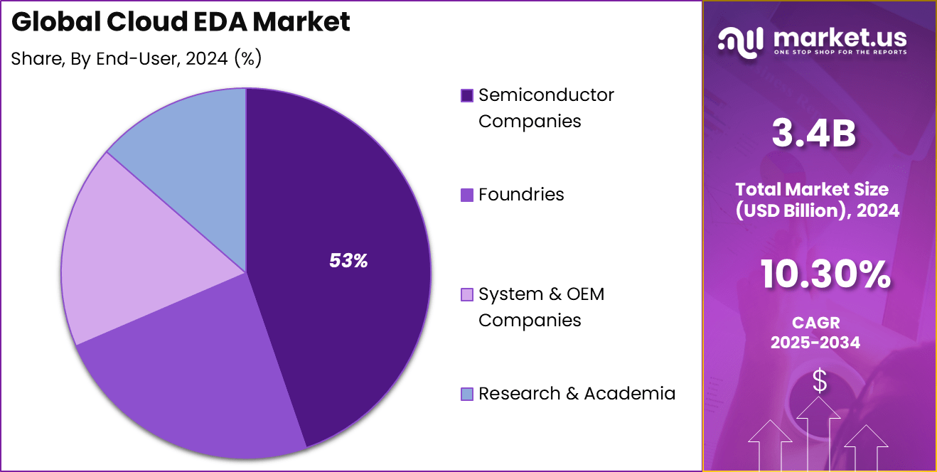
- By end-user, semiconductor companies captured 52.6%, relying on cloud EDA for faster and cheaper design work.
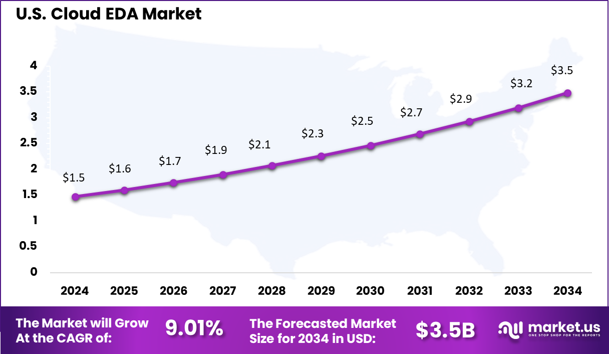
- North America had 48.2% of the global market, with the U.S. at USD 1.47 billion in 2025 and growing at a CAGR of 9.01%.
Role of Generative AI
Generative AI enhances cloud EDA by automating design processes through simulation and optimization of complex chip architectures. It generates realistic design variants and predicts outcomes, speeding up iterations in AI-driven verification tasks. Cloud platforms scale these AI models efficiently for real-time collaboration across global teams.
This integration reduces manual efforts in layout and testing by creating synthetic design data that mirrors real-world scenarios. Banks and tech firms benefit from faster time-to-market as generative AI handles intricate patterns in 5G and automotive chips. Overall, it boosts accuracy while lowering computational costs through on-demand cloud resources.
Tool Type Analysis
Simulation and analysis tools account for 38.9% of the Cloud EDA market, making them the most widely used tool category in cloud-based design environments. These tools are essential during early and mid stages of chip design, where engineers validate functionality, performance, and power behavior before physical fabrication. Cloud-based simulation enables faster testing of complex designs by providing access to scalable computing resources.
From a productivity standpoint, cloud simulation and analysis tools reduce design cycle time and support parallel testing. Design teams can run multiple simulations simultaneously without being limited by local hardware capacity. The strong share of this segment reflects the increasing complexity of semiconductor designs and the growing need for fast, accurate validation using flexible cloud infrastructure.
Organization Size Analysis
Large enterprises represent 71.3% of the Cloud EDA market, driven by their extensive chip development activities and large design teams. These organizations manage multiple design projects at the same time and require scalable resources to meet tight development schedules. Cloud EDA allows large enterprises to access high-performance computing without investing heavily in on-premises infrastructure.
Large enterprises also benefit from improved collaboration across global design teams. Cloud platforms enable shared access to tools and data, supporting faster decision-making and design iteration. The strong presence of this segment highlights how cloud EDA has become a strategic tool for managing complexity and scale in advanced semiconductor development.
End-User Analysis
Semiconductor companies account for 53% of end-user adoption, reflecting their direct dependence on advanced design automation tools. These companies use cloud EDA platforms to design, verify, and optimize integrated circuits for various applications. Cloud deployment helps them handle peak workloads during simulation and verification phases without long-term infrastructure commitments.
For semiconductor firms, cloud EDA supports faster innovation and improved cost efficiency. Design teams can scale resources as needed and focus more on design quality rather than infrastructure management. The strong share of semiconductor companies as end users highlights the growing acceptance of cloud-based EDA as a core part of modern chip design workflows.
Key Aspects of Cloud EDA
- Scalable Compute: Computing power can be increased or reduced as needed. This is useful for heavy tasks such as power analysis or verification, which need high processing capacity for short periods.
- Elastic Usage: Large and changing design workloads can be handled without buying expensive hardware in advance. This suits both small design teams and large semiconductor companies.
- SaaS Delivery Model: Many cloud EDA tools are offered through online platforms. This makes access easier and reduces the need for complex local installations.
- Team Collaboration: Design files and results can be shared securely across teams working in different locations. This supports better coordination and faster decision making.
- AI Support: Cloud platforms support AI based EDA tools that help improve chip design by optimizing power usage, performance, and area.
- Security and IP Protection: Strong security measures are provided by cloud and EDA vendors to protect sensitive design data and intellectual property.
Investment and Business Benefits
Rising demand from fabless firms and emerging regions like Asia-Pacific offers strong investment potential in Cloud EDA infrastructure. Providers can target tailored platforms for high-performance needs without fabrication facilities. Growth in AI chip design further expands opportunities for scalable solutions.
Cloud providers and EDA vendors investing in AI integrations and secure ecosystems stand to gain from startup funding and enterprise shifts. Hybrid workflows and sustainable design tools attract capital amid green computing trends. These areas promise long-term revenue through subscriptions and services.
Cloud EDA cuts operational costs by eliminating hardware maintenance and enabling efficient resource use during peak demands. Businesses achieve better budget control with flexible pricing, supporting projects without over-provisioning. This leads to predictable expenses and higher ROI on design efforts.
Improved productivity comes from real-time collaboration and faster simulations, shortening development timelines. Teams iterate designs more effectively, enhancing innovation in products like wearables and automotive systems. Overall, these benefits strengthen competitiveness in fast-paced industries.
Emerging Trends
Key Trend Description AI ML Design Tools AI accelerates chip design by improving layouts, identifying bugs early, and reducing overall design time. Hybrid Cloud Models A mix of on premises and cloud systems is used to balance performance, security, and flexibility. Real Time Team Work Global engineering teams collaborate on chip designs simultaneously through cloud platforms. Edge AI Auto Design Design tools focus on smaller chips used in vehicles, mobile devices, and edge computing. Green Cloud Power Energy efficient data centers support sustainable and eco friendly semiconductor design workflows. Growth Factors
Key Factors Description Complex Chip Needs Advanced nodes and complex architectures require high cloud computing power for simulations. Fast Market Time Cloud based design tools reduce the time needed to move from concept to manufacturing. Cost Pay as Go Cloud usage avoids heavy upfront infrastructure costs by paying only for required resources. Team Spread World Cloud platforms allow remote design teams to share files and work efficiently. AI Chip Boom Growth in AI, 5G, automotive, and mobile devices increases demand for cloud based EDA tools. Key Market Segments
By Tool Type
- Semiconductor IP
- IC Physical Design & Verification
- PCB & Multi-Chip Module Design
- Simulation & Analysis
- Others
By Organization Size
- Large Enterprises
- Small and Medium-sized Enterprises (SMEs)
By End-User
- Semiconductor Companies
- Foundries
- System & OEM Companies
- Research & Academia
Regional Analysis
North America accounted for 48.2% share, supported by strong concentration of semiconductor design firms, advanced foundry partnerships, and early adoption of cloud based engineering tools. Cloud EDA platforms have been adopted to handle growing design complexity, shorten chip development cycles, and support collaboration across distributed design teams.
Demand has been driven by rising investment in advanced node development, system on chip designs, and specialized processors for AI, automotive, and data center applications. The ability to scale computing resources on demand has made cloud EDA an attractive option for managing peak simulation and verification workloads.

The U.S. market reached USD 1.47 Bn and is projected to grow at a 9.01% CAGR, reflecting steady demand from both large semiconductor companies and emerging chip startups. Adoption has been supported by the need to reduce upfront infrastructure investment and accelerate time to market.
Cloud EDA platforms allow U.S. design teams to access high performance computing resources without maintaining expensive on premises systems, which is particularly valuable for verification and simulation intensive workloads.
Key Regions and Countries
- North America
- US
- Canada
- Europe
- Germany
- France
- The UK
- Spain
- Italy
- Russia
- Netherlands
- Rest of Europe
- Asia Pacific
- China
- Japan
- South Korea
- India
- Australia
- Singapore
- Thailand
- Vietnam
- Rest of APAC
- Latin America
- Brazil
- Mexico
- Rest of Latin America
- Middle East & Africa
- South Africa
- Saudi Arabia
- UAE
- Rest of MEA
Opportunities & Threats
The Cloud EDA market presents strong opportunities as semiconductor companies face rising design complexity and shorter development cycles. Cloud based EDA tools allow design teams to access high performance computing resources without investing heavily in on premises infrastructure.
This supports faster simulation, verification, and testing of advanced chip designs. Growing demand for AI processors, automotive electronics, and advanced nodes is increasing the need for scalable design environments that can handle large workloads efficiently.
The market faces threats related to data security and intellectual property protection. Semiconductor design data is highly sensitive, and concerns about data leakage or unauthorized access can limit cloud adoption. Regulatory requirements in some regions require strict data control, which may restrict where and how cloud EDA tools are deployed. These factors can slow adoption among risk averse organizations.
Another threat is performance reliability and network dependence. Design workloads require consistent high speed access, and any network disruption can affect productivity.Some companies also worry about long term cost visibility, as usage based pricing can become expensive for continuous large scale simulations. Vendor lock in and limited portability of design data between platforms further add to buyer hesitation.
Competitive Analysis
The competitive landscape of the cloud EDA market is shaped by established electronic design automation vendors alongside major cloud service providers. Synopsys, Inc., Cadence Design Systems, Inc., and Siemens AG through Mentor Graphics hold strong positions due to their comprehensive EDA portfolios and long standing relationships with semiconductor and system design companies.
ANSYS, Inc., Keysight Technologies, Inc., Altium, Ltd., Silvaco, Inc., and Zuken, Inc. strengthen competition by offering simulation, verification, PCB design, and mixed signal tools that are increasingly delivered through cloud based deployment models. IP focused players such as ARM, Ltd. and Xilinx under AMD support cloud EDA adoption by aligning design workflows with scalable compute and advanced silicon platforms.
Top Key Players in the Market
- Synopsys, Inc.
- Cadence Design Systems, Inc.
- Siemens AG (Mentor Graphics)
- ANSYS, Inc.
- Keysight Technologies, Inc.
- Altium, Ltd.
- Silvaco, Inc.
- Zuken, Inc.
- Xilinx, Inc. (AMD)
- ARM, Ltd.
- Google LLC
- Amazon Web Services, Inc.
- Microsoft Corporation
- IC Manage, Inc.
- ClioSoft, Inc.
- Others
Future Outlook
The future outlook for the Cloud EDA market is expected to remain strong as semiconductor design becomes more complex and resource intensive. Design teams are moving to cloud based EDA tools to access scalable compute power, reduce infrastructure costs, and speed up chip development cycles.
Cloud environments also support collaboration between distributed design teams, which is becoming common across global projects. In the coming years, tighter integration with AI driven design optimization, advanced verification, and secure cloud environments is likely to improve efficiency and reduce time to tape out.
Opportunities lie in
- Scalable compute for advanced chip design: Cloud platforms can support large simulations and verification workloads without heavy upfront investment.
- Collaboration for global design teams: Shared cloud environments can improve coordination and version control across locations.
- Support for startups and fabless firms: Cloud EDA lowers entry barriers by reducing the need for expensive on premises infrastructure.
Recent Developments
- July, 2025: Synopsys wrapped up its massive $35 billion acquisition of Ansys, blending top EDA tools with simulation strengths to target a $31 billion market and speed up AI-driven chip and system work.
- June, 2025: Siemens EDA launched its AI System at the Design Automation Conference, bringing generative and agentic AI to tools like Aprisa AI and Calibre Vision AI for faster semiconductor and PCB workflows, with cloud options.
Report Scope
Report Features Description Market Value (2024) USD 3.4 Bn Forecast Revenue (2034) USD 9 Bn CAGR(2025-2034) 10.30% Base Year for Estimation 2024 Historic Period 2020-2023 Forecast Period 2025-2034 Report Coverage Revenue forecast, AI impact on Market trends, Share Insights, Company ranking, competitive landscape, Recent Developments, Market Dynamics and Emerging Trends Segments Covered By Tool Type (Semiconductor IP, IC Physical Design & Verification, PCB & Multi-Chip Module Design, Simulation & Analysis, Others), By Organization Size (Large Enterprises, Small and Medium-sized Enterprises (SMEs)), By End-User (Semiconductor Companies, Foundries, System & OEM Companies, Research & Academia) Regional Analysis North America – US, Canada; Europe – Germany, France, The UK, Spain, Italy, Russia, Netherlands, Rest of Europe; Asia Pacific – China, Japan, South Korea, India, New Zealand, Singapore, Thailand, Vietnam, Rest of Latin America; Latin America – Brazil, Mexico, Rest of Latin America; Middle East & Africa – South Africa, Saudi Arabia, UAE, Rest of MEA Competitive Landscape Synopsys, Inc., Cadence Design Systems, Inc., Siemens AG (Mentor Graphics), ANSYS, Inc., Keysight Technologies, Inc., Altium, Ltd., Silvaco, Inc., Zuken, Inc., Xilinx, Inc. (AMD), ARM, Ltd., Google LLC, Amazon Web Services, Inc., Microsoft Corporation, IC Manage, Inc., ClioSoft, Inc., Others Customization Scope Customization for segments, region/country-level will be provided. Moreover, additional customization can be done based on the requirements. Purchase Options We have three license to opt for: Single User License, Multi-User License (Up to 5 Users), Corporate Use License (Unlimited User and Printable PDF)  Market") Cloud Electronic Design Automation (EDA) MarketPublished date: Dec. 2025add_shopping_cartBuy Now get_appDownload Sample
Cloud Electronic Design Automation (EDA) MarketPublished date: Dec. 2025add_shopping_cartBuy Now get_appDownload Sample -
-
- Synopsys, Inc.
- Cadence Design Systems, Inc.
- Siemens AG (Mentor Graphics)
- ANSYS, Inc.
- Keysight Technologies, Inc.
- Altium, Ltd.
- Silvaco, Inc.
- Zuken, Inc.
- Xilinx, Inc. (AMD)
- ARM, Ltd.
- Google LLC
- Amazon Web Services, Inc.
- Microsoft Corporation
- IC Manage, Inc.
- ClioSoft, Inc.
- Others
Our Clients
- 171258
- Dec. 2025