Global Chemical Mechanical Planarization Market Size, Share Analysis Report By Equipment (CMP Equipment, CMP Consumable, Pads, Others), By Application (Integrated Circuits, Compound Semiconductors, Mems and Nems, Others) , By Region and Companies - Industry Segment Outlook, Market Assessment, Competition Scenario, Trends and Forecast 2025-2034
- Published date: Oct 2025
- Report ID: 163108
- Number of Pages: 366
- Format:
-
keyboard_arrow_up
Quick Navigation
Report Overview
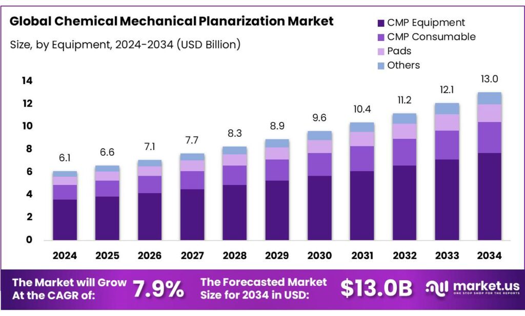
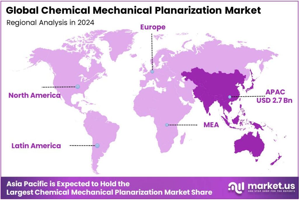
The Global Chemical Mechanical Planarization Market size is expected to be worth around USD 13.0 Billion by 2034, from USD 6.1 Billion in 2024, growing at a CAGR of 7.9% during the forecast period from 2025 to 2034. In 2024 Asia Pacific held a dominant market position, capturing more than a 45.9% share, holding USD 2.7 Billion in revenue.
Chemical Mechanical Planarization (CMP) sits at the heart of advanced wafer fabrication, enabling ultra-flat surfaces for multi-patterning, 3D NAND, and advanced packaging. CMP demand closely tracks wafer capacity and equipment outlays. SEMI projects global 300 mm fab equipment spending at $107 billion in 2025, rising to $116 billion in 2026 and $120 billion in 2027, a capex cadence that underpins robust consumables pull for slurries, pads, and conditioners.
- In parallel, SEMI expects front-end fab equipment to reach $110 billion in 2025, marking a sixth straight year of growth—another signal of sustained CMP tool and consumable utilization. Wafer fundamentals are also improving: global silicon wafer shipments are projected to climb 5.4% in 2025 to 12,824 MSI, with a new record expected by 2028—directly supportive of higher polish volumes.
The industrial backdrop is reinforced by policy and megaprojects. In the U.S., the CHIPS Act provides $50 billion, including $39 billion in direct incentives for fabs, packaging, and equipment, catalyzing domestic capacity additions that require extensive CMP steps. TSMC’s Arizona site illustrates the scale: an initial $65 billion program now accompanied by plans to invest an additional $100 billion in the U.S., with a preliminary $6.6 billion federal funding agreement—each dollar of new wafer capacity multiplying downstream CMP demand. Europe’s Chips Act adds €43 billion in public investment through 2030, supporting new EU capacity and localization of advanced nodes, again CMP-intensive.
Key driving factors for CMP demand in 2025–2028 include node migration and packaging. SEMI expects WFE growth to continue into $122.1 billion by 2026, while global 300 mm spending is projected to trend up again after 2026; combined with a capacity build that industry trackers estimate at ~33.6 million wafers/month in 2025, this points to sustained CMP step counts for copper/low-k, tungsten/cobalt liners, STI, and dielectric layers, plus aggressive post-CMP cleans. Energy-intense enablers compound flattening requirements; each EUV scanner can draw ~1 MW of electricity, sharpening the need for CMP process efficiency and lower-consumption tools.
Energy and utilities are central to CMP’s industrial footprint. The International Energy Agency (IEA) estimates that about 60% of semiconductor product manufacturing energy is tied to wafer and semiconductor production processes, with 40% used for facility auxiliaries such as ultrapure water and cooling—systems intimately linked to CMP slurries, rinses, and post-CMP cleans. In parallel, the IEA projects global electricity for data centres to rise from ~460 TWh in 2024 to >1,000 TWh by 2030, reinforcing multi-year capacity builds that flow through to CMP steps.
- Government programs amplify the cycle. In the United States, the CHIPS and Science Act totals $52 billion, with $36 billion+ in funding announcements and named grants including up to $325 million for Hemlock Semiconductor (hyper-pure polysilicon) and up to $125 million for GlobalFoundries—cascading support for upstream materials and fab expansions that ultimately add CMP load. In Europe, the EU Chips Act mobilizes >€43 billion by 2030, matched by private investment and aimed at securing leading-edge and specialty capacity across the value chain.
Key Takeaways
- Chemical Mechanical Planarization Market size is expected to be worth around USD 13.0 Billion by 2034, from USD 6.1 Billion in 2024, growing at a CAGR of 7.9%.
- CMP Equipment held a dominant market position, capturing more than a 58.9% share of the overall Chemical Mechanical Planarization market.
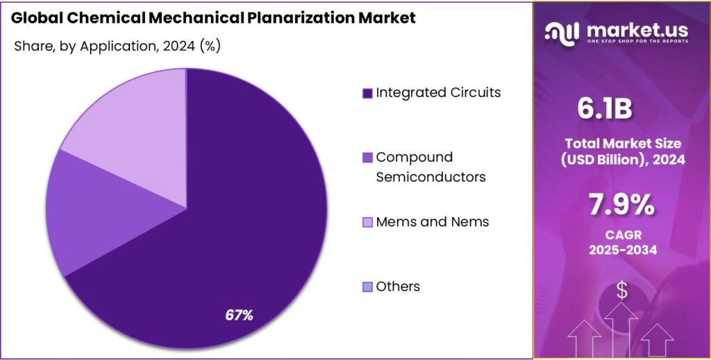
- Integrated Circuits held a dominant market position, capturing more than a 67.1% share of the overall Chemical Mechanical Planarization (CMP) market.
- Asia Pacific emerged as the leading region in the Chemical Mechanical Planarization (CMP) market, accounting for 45.9% of the global share, valued at approximately USD 2.7 billion.
By Equipment Analysis
CMP Equipment dominates with 58.9% share due to increasing semiconductor fabrication demand
In 2024, CMP Equipment held a dominant market position, capturing more than a 58.9% share of the overall Chemical Mechanical Planarization market. This growth was mainly supported by the rapid expansion of semiconductor manufacturing facilities and the rising adoption of advanced node technologies. CMP equipment, which includes polishing tools, platen systems, and cleaning stations, plays a critical role in achieving wafer planarity during chip fabrication. The demand for these tools surged in 2024 as major foundries and integrated device manufacturers expanded their production lines to meet the increasing global chip demand.
CMP equipment utilization increased notably across Asia-Pacific, especially in Taiwan, South Korea, and China, where large fabrication plants continue to drive global supply. By 2025, this equipment segment is expected to maintain its lead, supported by the ongoing adoption of 3D NAND and advanced packaging technologies, which require multiple CMP steps for each wafer layer.
By Application Analysis
Integrated Circuits dominate with 67.1% share driven by advanced chip manufacturing growth
In 2024, Integrated Circuits held a dominant market position, capturing more than a 67.1% share of the overall Chemical Mechanical Planarization (CMP) market. The segment’s leadership was largely driven by the increasing production of high-performance chips used in smartphones, data centers, electric vehicles, and artificial intelligence systems. CMP plays a crucial role in integrated circuit fabrication, as it ensures the wafer’s surface uniformity during multiple metal and dielectric layer depositions, which is essential for advanced node technologies below 7 nm.
The rapid expansion of global semiconductor manufacturing capacity in 2024 significantly boosted CMP demand within integrated circuit applications. Foundries and logic manufacturers across Asia-Pacific, including Taiwan, South Korea, and China, were among the primary contributors to this growth. As device miniaturization continues and chip architectures become more complex, the need for highly precise planarization has risen sharply. This trend is expected to continue in 2025, supported by strong investment in AI-driven processors and 3D NAND memory production, both of which require multiple CMP steps to achieve desired device performance.
Key Market Segments
By Equipment
- CMP Equipment
- Single-Wafer CMP Systems
- Post-CMP Cleaning Equipment
- Batch CMP Systems
- Others
- CMP Consumable
- CMP Slurry
- Silica-Based Slurry
- Aluminum Oxide-Based Slurry
- Cerium Oxide-Based Slurry
- Composite/Engineered Abrasive Slurry
- Others
- Pads
- Others
By Application
- Integrated Circuits
- Compound Semiconductors
- Mems and Nems
- Others
Emerging Trends
Hybrid bonding & 3D packaging are reshaping CMP right now
A clear, latest trend in chemical mechanical planarization (CMP) is its fast shift from “planarize-and-move-on” to precision surfaces for hybrid bonding and dense 2.5D/3D packages. As chipmakers stack logic with HBM and chiplets, every added interface needs flatter, cleaner surfaces, tighter within-wafer non-uniformity, and low defectivity—driving new slurries, pads, and endpoint control.
- The International Energy Agency (IEA) projects global data-centre electricity use to roughly double to ~945 TWh by 2030, propelled by AI. This signals durable demand for AI chips and memory that rely on hybrid bonding—and thus on CMP that can reliably deliver atomic-scale flatness before bond.
Public programs are accelerating the trend from lab to high-volume. In the United States, the Department of Commerce’s CHIPS R&D National Advanced Packaging Manufacturing Program (NAPMP) moved from intent to awards: a Notice of Intent signalled up to $1.55 billion for packaging R&D areas (chiplets, photonics/connector tech, thermal, EDA co-design), then final awards of $1.4 billion were announced in January 2025 to stand up domestic advanced-packaging capabilities. Both steps push hybrid bonding and associated CMP modules into manufacturable reality. Earlier, NIST also launched up to $300 million for advanced-packaging research projects, again strengthening the ecosystem that depends on repeatable CMP at bonding surfaces.
Drivers
Packaging & Advanced Integration Spur Demand
One major driving factor for the chemical mechanical planarization (CMP) market is the explosive growth in advanced packaging and integration demands driven by artificial-intelligence (AI) and high-performance compute systems. As companies build more intricate stacks of logic, memory and interposers, the requirement for ultra-flat surfaces across multilayer wafers becomes non-negotiable — and that is where CMP plays a pivotal role.
- The International Energy Agency (IEA) estimates that global electricity consumption by data centres alone will rise from approximately 415 terawatt-hours (TWh) in 2024 — already about 1.5% of global electricity consumption — to around 945 TWh by 2030. This massive growth in data-centres and high-intensity computing reflects the backend demand for chips, packaging, and interconnects.
Moreover, the advanced packaging trend is gaining full force: As reported by industry media, “the fast adoption of chiplets will continue to drive wafer-level packaging (WLP) growth in 2025”. The more complex the packaging, the more surfaces need to be planarised to meet overlay and defect control standards, hence CMP is indispensable. Furthermore, global semiconductor equipment spending is projected to reach about US$111 billion in 2025, with a further rise to around US$122 billion in 2026. These broad fab and assembly investments feed directly into increased CMP tool and consumable demand.
Government initiatives are amplifying these structural flows. In many jurisdictions, incentives and subsidies for domestic chip manufacturing, packaging, and assembly create new fab projects, test/pack facilities and multiple layers of interconnect. Each new advanced-package line implies CMP demand. For example, as countries push AI infrastructure and memory stacks, the downstream CMP steps gain urgency.
Restraints
Resource-Intensity Risks Highlighting a Key Restraining Factor
One significant restraining factor for the chemical mechanical planarization (CMP) process is the intense consumption of ultrapure water and associated treatment energy, which raises environmental, regulatory and cost pressures for fabs and CMP-tool/consumable suppliers.
- For example, the International Energy Agency notes that a single advanced semiconductor manufacturing facility can use about 10 million gallons of ultrapure water per day — a volume equivalent to the daily water use of roughly 33,000 U.S. households. A related report found that across 27 major semiconductor manufacturers, ultrapure-water usage reached about 551 million m³ in 2022.
Moreover, the energy-water nexus makes things more complex. Ultrapure water production is energy-intensive: treating municipal-grade water into the purity required for wafers consumes substantial electricity, and much of the discharge from CMP and rinses must be treated or recycled, further raising energy and capital-cost burdens. One discussion describes the mirrored increase in both water withdrawal and energy consumption for semiconductor companies between 2017–2021, with final energy use rising ~8.9% per annum and water usage ~6.1% for a sample of Taiwanese electronics companies.
These resource-intensive demands for CMP escalate especially in advanced packaging and high-density interconnects where multiple CMP steps are required (metals, dielectrics, bond interfaces). As the number of layers rises, so do rinse and clean cycles, pad wear and consumable throughput, which scales up the resource burden. In a real-world sense, this means a micro-layer polishing step isn’t just adding cost per part — it’s also adding thousands of litres of high-cost water, kWs of power, and (in some jurisdictions) risk of regulatory fines or scarce water supply.
For example, one fab in Arizona plans to reclaim about 65% of the water used in its facility. The regulatory implications are also real: in many semiconductor-hub regions governments are tightening water-permit regimes, pushing for water-efficiency benchmarking and even linking manufacturing expansion to sustainable water use.
Opportunity
Advanced packaging & AI infrastructure: the next big opening for CMP
A powerful growth opportunity for chemical mechanical planarization (CMP) sits in the rapid build-out of AI and high-performance computing infrastructure, which depends on denser 2.5D/3D packaging, HBM stacks, and hybrid bonding—each step demanding ultra-flat surfaces. The International Energy Agency projects global electricity used by data centres will roughly double to ~945 TWh by 2030 (Base Case), signalling sustained investment in AI chips and memory that pull through multiple CMP steps across metals, dielectrics, and bonding interfaces.
- This demand wave is already visible in equipment spending: industry association SEMI forecasts total semiconductor equipment sales of $125.5 billion in 2025, with back-end assembly/packaging equipment up 7.7% to $5.4 billion and test at a record $9.3 billion—a backdrop that expands CMP tools and consumables alongside deposition, etch, and lithography.
Public policy adds momentum and creates local market openings. In the United States, the CHIPS and Science Act provides $50 billion for semiconductor R&D, incentives, and metrology, including a National Advanced Packaging Program that aligns directly with CMP-intensive flows. In Europe, the European Chips Act mobilizes over €43 billion in public policy-driven investment through 2030, with additional private capital expected—supporting new fabs, specialty nodes, and advanced packaging sites that raise CMP step counts.
For CMP suppliers, the opportunity is not only volume, but value. Tool makers and consumables vendors can differentiate with high-selectivity slurries tuned for cobalt, ruthenium and hybrid-bond oxide surfaces; low-downforce pads that protect fragile stacks; and endpoint control that shortens polish time while tightening within-wafer non-uniformity. Sustainability features increasingly determine wins: fabs seek measurable cuts in energy and water per polish, and in oxidizer loadings and waste.
As AI data-centre growth accelerates, utilities and governments will tighten sustainability requirements; vendors who can document lower kWh/wafer and L/wafer at identical removal rates will align with both CHIPS and EU policy priorities while reducing fab operating costs. On the demand side, the IEA notes the United States will account for the largest share of the data-centre electricity increase by 2030, with the EU and China also significant—creating multi-region sales pipelines for CMP platforms and consumables.
Regional Insights
Asia Pacific leads the Chemical Mechanical Planarization market with 45.9% share valued at USD 2.7 billion
In 2024, Asia Pacific emerged as the leading region in the Chemical Mechanical Planarization (CMP) market, accounting for 45.9% of the global share, valued at approximately USD 2.7 billion. The region’s dominance is primarily driven by the strong presence of semiconductor manufacturing hubs across China, Taiwan, South Korea, and Japan, which together contribute more than 70% of global semiconductor wafer fabrication capacity. Rapid industrialization, government-backed semiconductor development initiatives, and increasing capital expenditure from leading foundries have strengthened CMP adoption in the region.
Countries such as Taiwan and South Korea, home to major chip producers like TSMC and Samsung Electronics, significantly boosted their wafer production in 2024, directly driving CMP equipment and consumable demand. China also expanded its domestic semiconductor production under national initiatives like the Made in China 2025 plan, aimed at increasing self-sufficiency in chip manufacturing. This has led to substantial investments in CMP tools and materials to support advanced process technologies below 10 nm.
Key Regions and Countries Insights
- North America
- US
- Canada
- Europe
- Germany
- France
- The UK
- Spain
- Italy
- Rest of Europe
- Asia Pacific
- China
- Japan
- South Korea
- India
- Australia
- Rest of APAC
- Latin America
- Brazil
- Mexico
- Rest of Latin America
- Middle East & Africa
- GCC
- South Africa
- Rest of MEA
Key Players Analysis
Applied Materials Inc.: Applied Materials has long been a dominant supplier of CMP equipment, especially for advanced logic and memory manufacturing. For example, its “Opta™ CMP” platform is described as offering high throughput density and flexibility across metal and non-metal applications. The company leverages its global installed base (over 2,000 systems shipped historically) to continue pushing process control and uniformity improvements.
Ebara Corporation: Japan’s Ebara has established itself as a global leader in CMP systems via its Systems Equipment Division. It supplies CMP tools across 200 mm and 300 mm wafers and has delivered over 3,000 units cumulatively. The company’s technology is also being positioned for panel-level organic interposer applications through collaborative consortia.
DuPont de Nemours Inc.: DuPont is a leading consumables supplier in the CMP market, offering a broad pad and slurry portfolio for advanced nodes. Its “Ikonic™ 9000” pad series recently received industry recognition for AI-driven semiconductor manufacturing enhancements. DuPont emphasises materials science innovation, longer pad lifetime, and support for sub-14 nm as well as 3D-IC technologies.
Top Key Players Outlook
- Applied Materials Inc.
- Entegris Inc.
- Ebara Corporation
- Lapmaster Wolters Gmbh
- Dupont De Nemours Inc.
- Fujimi Incorporated
- Revasum Inc.
- Resonac Holdings Corporation
- Okamoto Corporation
- Fujifilm Corporation
- Tokyo Seimitsu Co. Ltd
Recent Industry Developments
March 31, 2024 Fujimi Incorporated, reported net sales of ¥51,423 million, down from ¥58,394 million the previous year, representing an 11.9% decline.
In 2024, DuPont reported net sales of USD 12,386 million, up 3 % from the previous year, with operating EBITDA of USD 3,144 million, representing a margin of 25.4%.
Report Scope
Report Features Description Market Value (2024) USD 6.1 Bn Forecast Revenue (2034) USD 13.0 Bn CAGR (2025-2034) 7.9% Base Year for Estimation 2024 Historic Period 2020-2023 Forecast Period 2025-2034 Report Coverage Revenue Forecast, Market Dynamics, Competitive Landscape, Recent Developments Segments Covered By Equipment (CMP Equipment, CMP Consumable, Pads, Others), By Application (Integrated Circuits, Compound Semiconductors, Mems and Nems, Others) Regional Analysis North America – US, Canada; Europe – Germany, France, The UK, Spain, Italy, Rest of Europe; Asia Pacific – China, Japan, South Korea, India, Australia, Singapore, Rest of APAC; Latin America – Brazil, Mexico, Rest of Latin America; Middle East & Africa – GCC, South Africa, Rest of MEA Competitive Landscape Applied Materials Inc., Entegris Inc., Ebara Corporation, Lapmaster Wolters Gmbh, Dupont De Nemours Inc., Fujimi Incorporated, Revasum Inc., Resonac Holdings Corporation, Okamoto Corporation, Fujifilm Corporation, Tokyo Seimitsu Co. Ltd Customization Scope Customization for segments, region/country-level will be provided. Moreover, additional customization can be done based on the requirements. Purchase Options We have three licenses to opt for: Single User License, Multi-User License (Up to 5 Users), Corporate Use License (Unlimited User and Printable PDF)  Chemical Mechanical Planarization MarketPublished date: Oct 2025add_shopping_cartBuy Now get_appDownload Sample
 -
-
- Applied Materials Inc.
- Entegris Inc.
- Ebara Corporation
- Lapmaster Wolters Gmbh
- Dupont De Nemours Inc.
- Fujimi Incorporated
- Revasum Inc.
- Resonac Holdings Corporation
- Okamoto Corporation
- Fujifilm Corporation
- Tokyo Seimitsu Co. Ltd
Our Clients
- 163108
- Oct 2025