Global Atomic Layer Deposition Equipment Market Size, Share, Growth Analysis By Equipment Type (Thermal ALD, Plasma-Enhanced ALD, Spatial ALD, Roll-to-Roll/Sheet-to-Sheet ALD, Others), By Substrate Size (300 mm, ≤ 200 mm, ≥ 450 mm), By Film Type (Oxide, Metal, Sulfide, Nitride, Fluoride), By Application (Electronics & Semiconductors, Healthcare & Biomedical, Energy & Power, Automotive, Data Centers, Others), By Region and Companies - Industry Segment Outlook, Market Assessment, Competition Scenario, Statistics, Trends and Forecast 2026-2035
- Published date: Jan 2026
- Report ID: 175839
- Number of Pages: 300
- Format:
-
keyboard_arrow_up
Quick Navigation
Report Overview
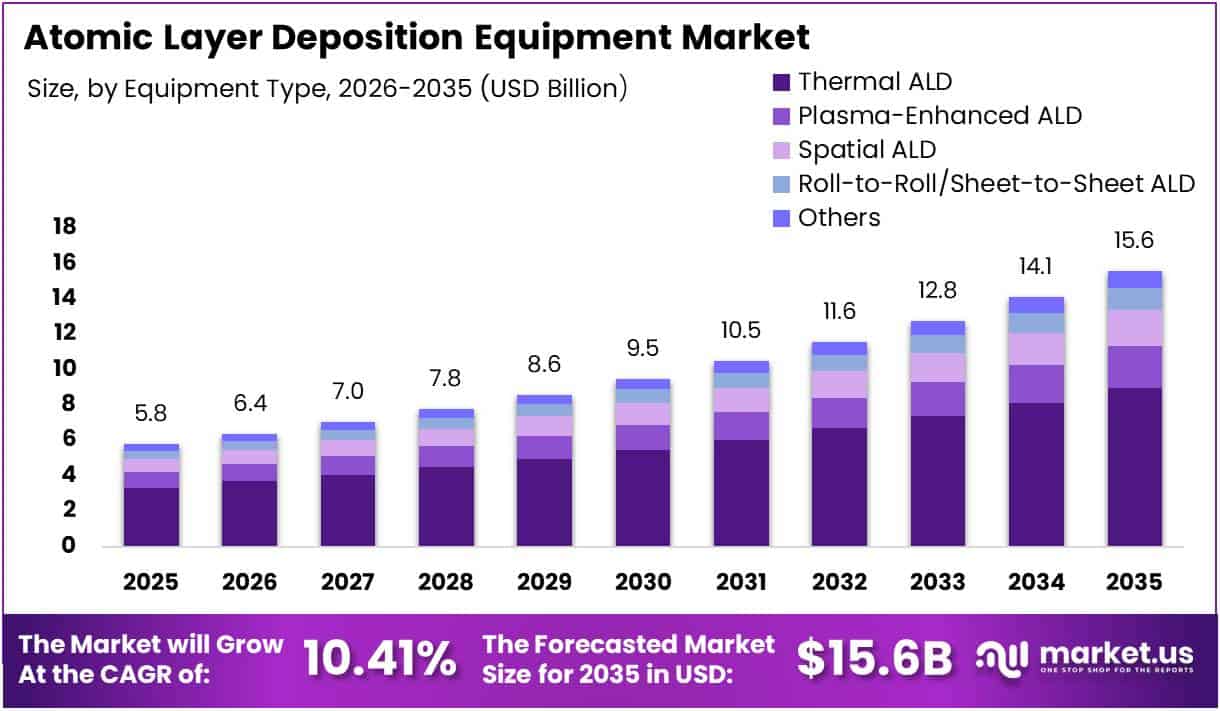
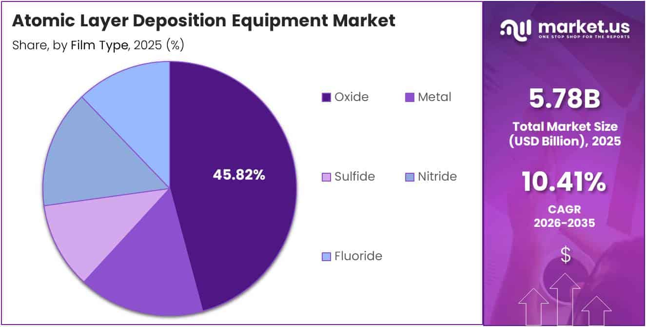
The Global Atomic Layer Deposition Equipment Market size is expected to be worth around USD 15.6 Billion by 2035 from USD 5.78 Billion in 2025, growing at a CAGR of 10.41% during the forecast period 2026 to 2035.
Atomic Layer Deposition Equipment represents advanced manufacturing systems that enable precise, nanoscale thin-film coating on various substrates. These sophisticated tools utilize sequential, self-limiting chemical reactions to deposit uniform material layers with atomic-level thickness control. Consequently, ALD technology has become indispensable in semiconductor fabrication and emerging applications.
The market experiences robust expansion driven by miniaturization trends in electronics and increasing complexity of semiconductor architectures. Moreover, the transition toward sub-10 nm technology nodes demands exceptional conformality and thickness uniformity that only ALD processes can deliver. Therefore, semiconductor manufacturers prioritize ALD equipment investments for next-generation device production.
Advanced logic chips, 3D NAND flash memory, and cutting-edge DRAM production increasingly rely on ALD technology for critical process steps. Additionally, high-aspect-ratio structures in FinFET transistors and vertical NAND architectures require ALD’s unique conformal coating capabilities. This technological necessity creates sustained demand across multiple semiconductor segments.
Government initiatives supporting semiconductor manufacturing expansion and domestic chip production capabilities further accelerate market growth. Furthermore, substantial investments in cleanroom infrastructure and advanced fabrication facilities drive ALD equipment adoption. Various national strategies prioritize semiconductor self-sufficiency, creating favorable regulatory environments for equipment procurement.
The healthcare and biomedical sectors present emerging opportunities as ALD enables precise surface modification for medical devices and implants. Similarly, energy storage applications benefit from ALD-coated battery electrodes that enhance performance and longevity. These diversification trends expand the addressable market beyond traditional semiconductor applications.
According to GreyB, Atomic Layer Deposition enables precise control of electrode surface chemistry at the nanoscale, with coating thicknesses ranging from 10-30 nanometers. Additionally, according to Oxford Academic, the etching rate for non-ideal ALD deposited Al₂O₃ films reached approximately 5.19 nm/min versus 1.11 nm/min for ideal processed films, indicating process design’s impact on etch resistance and film integrity.
According to Research, ultrathin ALD alumina coverage improved coverage uniformity to approximately 87.46% coverage at approximately 0.75 nm, rising to approximately 98.03% at approximately 2 nm. This data illustrates how precise ALD control affects functional film continuity and demonstrates the technology’s critical role in achieving desired material properties.
Key Takeaways
- Global Atomic Layer Deposition Equipment Market valued at USD 5.78 Billion in 2025, projected to reach USD 15.6 Billion by 2035
- Market growing at CAGR of 10.41% during forecast period 2026-2035
- Thermal ALD equipment dominates by equipment type segment with 57.80% market share
- 300 mm substrate size leads with 69.31% share in substrate size segment
- Oxide film type captures 45.82% share in film type segmentation
- Electronics & Semiconductors application holds commanding 86.24% market share
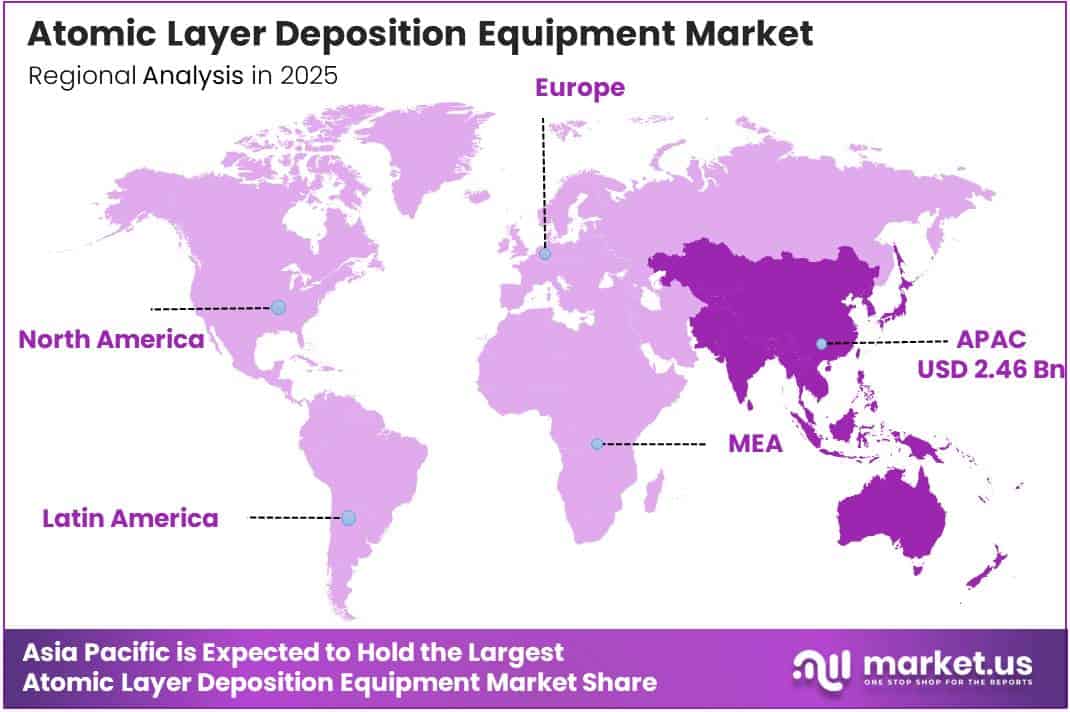
- Asia-Pacific region dominates with 42.70% share, valued at USD 2.46 Billion
Equipment Type Analysis
Thermal ALD dominates with 57.80% due to superior conformality and material versatility.
In 2025, Thermal ALD held a dominant market position in the By Equipment Type segment of Atomic Layer Deposition Equipment Market, with a 57.80% share. Thermal ALD systems utilize temperature-activated chemical reactions to deposit films with exceptional uniformity across complex three-dimensional structures. Their proven reliability in high-volume manufacturing and broad material compatibility make them the preferred choice for critical semiconductor applications.
Plasma-Enhanced ALD systems enable lower-temperature processing and expanded material options through plasma activation of precursor molecules. These tools prove essential for temperature-sensitive substrates and applications requiring enhanced film properties. Moreover, plasma-enhanced processes accelerate deposition rates while maintaining atomic-level precision, addressing throughput concerns in volume manufacturing environments.
Spatial ALD technology separates precursor exposure zones spatially rather than temporally, significantly improving throughput compared to conventional temporal ALD systems. This innovative approach moves substrates through sequential reaction chambers, enabling continuous processing. Consequently, spatial ALD attracts growing interest for applications balancing precision requirements with manufacturing efficiency demands.
Roll-to-Roll/Sheet-to-Sheet ALD enables continuous processing of flexible substrates for large-area applications beyond traditional semiconductor wafers. These platforms move substrates through sequential deposition zones, supporting high-volume production of displays, solar cells, and barrier coatings. Industrial applications include moisture barriers in flexible packaging and encapsulation layers for organic electronics.
Others category encompasses specialized configurations including fluidized bed reactors for powder coating and rotary spatial ALD for cylindrical substrates. These niche systems serve catalysis, pharmaceutical coatings, and advanced materials research. University research groups utilize customized ALD platforms for fundamental studies beyond conventional semiconductor applications.
Substrate Size Analysis
300 mm substrate size dominates with 69.31% due to industry standardization and economies of scale.
In 2025, 300 mm held a dominant market position in the By Substrate Size segment of Atomic Layer Deposition Equipment Market, with a 69.31% share. The 300 mm wafer format represents the current industry standard for advanced logic and memory production, offering optimal balance between manufacturing efficiency and capital investment. Leading semiconductor fabs globally utilize this substrate size for cutting-edge node production.
≤ 200 mm substrate equipment serves legacy device production, specialty semiconductor applications, and research institutions requiring smaller-scale processing capabilities. These systems maintain relevance for compound semiconductors, power devices, and MEMS applications. Additionally, research and development activities often utilize smaller substrate formats for process development and material exploration.
≥ 450 mm substrate tools represent the next-generation wafer size transition aimed at further improving manufacturing economics and chip output per wafer. However, industry adoption faces challenges including substantial infrastructure investments and equipment ecosystem development requirements. Nevertheless, development continues for future high-volume production scenarios.
Film Type Analysis
Oxide films dominate with 45.82% due to extensive use in gate dielectrics and passivation layers.
In 2025, Oxide held a dominant market position in the By Film Type segment of Atomic Layer Deposition Equipment Market, with a 45.82% share. Oxide materials including aluminum oxide, hafnium oxide, and silicon dioxide serve critical functions in transistor gate stacks, capacitor dielectrics, and protective passivation layers. Their excellent insulating properties and thermal stability make oxide ALD processes indispensable across semiconductor manufacturing.
Metal films deposited via ALD enable advanced metallization schemes, diffusion barriers, and seed layers for interconnect structures. Tungsten, copper, and ruthenium ALD processes address shrinking feature sizes where conventional deposition methods struggle. Moreover, metal ALD provides superior step coverage in high-aspect-ratio vias and trenches essential for three-dimensional device architectures.
Sulfide films enable photovoltaic applications, particularly for thin-film solar cells and buffer layers in CIGS devices. Metal sulfide materials serve as solid-state electrolytes in emerging battery technologies and chalcogenide semiconductors in phase-change memory. ALD sulfide processes benefit from excellent conformality for nanostructured photovoltaic architectures.
Nitride films including silicon nitride, titanium nitride, and aluminum nitride serve as diffusion barriers, etch stop layers, and hardmasks in semiconductor manufacturing. Titanium nitride ALD enables conformal electrode formation in DRAM capacitors requiring work function engineering. Aluminum nitride serves thermal management applications in power electronics and piezoelectric devices.
Fluoride materials provide unique optical properties, low refractive indices, and chemical resistance for specialized coating applications. Calcium fluoride and magnesium fluoride films serve as anti-reflective coatings for optical components and protective layers for UV lithography optics. The hydrophobic nature makes them attractive for microfluidic devices and anti-fouling coatings.
Application Analysis
Electronics & Semiconductors dominates with 86.24% due to indispensable role in advanced chip manufacturing.
In 2025, Electronics & Semiconductors held a dominant market position in the By Application segment of Atomic Layer Deposition Equipment Market, with an 86.24% share. Semiconductor fabrication requires ALD for high-k dielectrics, metal gates, spacers, and numerous other critical process steps in logic and memory production. The relentless scaling of transistor dimensions and increasing architectural complexity ensure sustained ALD equipment demand within this sector.
Healthcare & Biomedical applications leverage ALD for biocompatible coatings on implants, drug delivery systems, and diagnostic devices requiring precise surface modification. The technology enables controlled functionalization of medical device surfaces, improving biointegration and performance. Additionally, ALD coatings enhance corrosion resistance and antimicrobial properties of surgical instruments and implantable electronics.
Energy & Power sectors utilize ALD for battery electrode coatings, fuel cell components, and photovoltaic devices. ALD coatings on battery electrodes improve cycle life and suppress side reactions. Solid-state batteries benefit from uniform electrolyte layer deposition. Solar cells achieve efficiency improvements through ALD passivation layers and transparent conductive oxides.
Automotive applications incorporate ALD for advanced driver assistance systems, LiDAR sensors, power electronics, and electric vehicle battery components. ALD coatings on power devices improve thermal management and breakdown voltage characteristics critical for electric vehicle powertrains. Sensor applications benefit from precise optical coating capabilities for cameras and autonomous vehicle systems.
Data Centers drive demand through high-performance computing processors, AI accelerators, and high-bandwidth memory technologies enabling cloud computing workloads. Advanced logic chips utilize multiple ALD process steps for gate stacks and interconnects. High-bandwidth memory stacks require ALD for through-silicon vias and interposer metallization schemes.
Others encompasses aerospace components, decorative coatings, and cultural heritage preservation applications. Aerospace utilizes ALD for protective coatings on turbine components and satellite electronics. Research institutions explore ALD for catalysis development, MEMS devices, and novel device architectures beyond current commercial applications.
Key Market Segments
By Equipment Type
- Thermal ALD
- Plasma-Enhanced ALD
- Spatial ALD
- Roll-to-Roll/Sheet-to-Sheet ALD
- Others
By Substrate Size
- 300 mm
- ≤ 200 mm
- ≥ 450 mm
By Film Type
- Oxide
- Metal
- Sulfide
- Nitride
- Fluoride
By Application
- Electronics & Semiconductors
- Healthcare & Biomedical
- Energy & Power
- Automotive
- Data Centers
- Others
Drivers
Rising Demand for Sub-10 nm Semiconductor Nodes Requiring Atomic-Scale Film Control Drives Market Growth
Advanced semiconductor manufacturing increasingly relies on technology nodes below 10 nanometers, where conventional deposition techniques cannot achieve required precision and uniformity. ALD equipment uniquely delivers atomic-level thickness control and exceptional conformality essential for gate dielectrics, spacers, and interconnect barriers. Consequently, every leading-edge chip fabrication facility requires multiple ALD systems to meet stringent process specifications and yield targets.
The proliferation of high-aspect-ratio structures in FinFET transistors and gate-all-around architectures demands conformal coating capabilities that only ALD processes provide. Moreover, multi-patterning schemes and extreme ultraviolet lithography integration necessitate precise thin-film deposition for pattern transfer and hardmask applications. Therefore, semiconductor manufacturers continuously invest in advanced ALD equipment to enable next-generation device production.
Memory device evolution toward three-dimensional NAND architectures with 200+ layers and advanced DRAM capacitor designs creates substantial ALD equipment demand. Additionally, the transition to high-k metal gate technology across all logic platforms mandates ALD for critical dielectric and electrode depositions. These technological imperatives ensure sustained equipment procurement across the semiconductor industry.
Restraints
Process Complexity and Limited Material Compatibility Across Certain Precursors Limit Market Adoption
ALD processes require sophisticated process optimization involving precise temperature control, precursor dosing, and purge cycle management that demand specialized expertise. Furthermore, precursor chemistry development for specific materials remains challenging, with limited commercially available options for certain film compositions. This complexity increases implementation barriers for smaller manufacturers and emerging application areas lacking established process recipes.
Material compatibility issues arise when certain precursors demonstrate instability, toxicity concerns, or incompatibility with existing fab infrastructure and environmental safety systems. Additionally, some desired film properties require exotic precursor molecules with high costs or limited supply availability. These constraints restrict ALD adoption in price-sensitive applications and create dependencies on specialized chemical suppliers.
The slower deposition rates inherent to ALD’s sequential, self-limiting reaction mechanism present throughput challenges compared to chemical vapor deposition and physical vapor deposition alternatives. Moreover, batch processing limitations and chamber conditioning requirements extend overall process times. Consequently, applications tolerating lower conformality may favor faster conventional deposition methods, particularly in high-volume manufacturing scenarios prioritizing cost per wafer.
Growth Factors
Accelerating Use of ALD in Battery Electrodes and Solid-State Energy Storage Creates Expansion Opportunities
Energy storage applications increasingly adopt ALD technology for electrode surface modification that enhances battery performance, cycle life, and safety characteristics. Ultrathin ALD coatings on cathode and anode materials suppress unwanted side reactions and improve ionic conductivity at material interfaces. Therefore, battery manufacturers invest in ALD equipment to develop next-generation lithium-ion and solid-state battery technologies with superior energy density.
Solid-state battery development particularly benefits from ALD’s capability to deposit uniform solid electrolyte layers and protective interlayers with precise thickness control. Additionally, ALD enables surface engineering of high-capacity electrode materials that otherwise suffer from structural degradation during charge-discharge cycling. These performance improvements drive equipment adoption across battery research institutions and manufacturing facilities.
Automotive electronics and power device markets create substantial growth opportunities as electric vehicles and renewable energy systems demand advanced semiconductor components. Moreover, ALD processes enhance power device reliability through improved dielectric quality and interface engineering. Data center expansion for artificial intelligence and cloud computing workloads further accelerates demand for ALD-enabled advanced logic and high-bandwidth memory chips.
Emerging Trends
Shift Toward Spatial ALD Systems for Higher Throughput Manufacturing Reshapes Technology Landscape
Industry focus intensifies on spatial ALD architectures that overcome traditional temporal ALD throughput limitations through continuous substrate movement across separated reaction zones. These innovative systems demonstrate potential for 10x throughput improvements while maintaining atomic-level deposition control. Consequently, equipment manufacturers develop spatial ALD tools targeting applications where throughput directly impacts manufacturing economics without compromising film quality requirements.
Integration of ALD with atomic layer etching capabilities in unified process platforms enables novel device fabrication approaches and reduces substrate handling complexity. Furthermore, combined deposition-etch sequences allow precise feature shaping and surface engineering impossible with separate tools. This convergence trend drives development of multi-functional process chambers optimizing fab footprint utilization and process flow efficiency.
Low-temperature ALD process development accelerates to address flexible electronics, organic device fabrication, and temperature-sensitive substrate applications. Additionally, precursor chemistry innovations enable film deposition at temperatures below 100°C without sacrificing film quality. These advancements expand ALD’s addressable market beyond traditional rigid semiconductor substrates into emerging flexible display, wearable sensor, and printed electronics applications.
Regional Analysis
Asia-Pacific Dominates the Atomic Layer Deposition Equipment Market with a Market Share of 42.70%, Valued at USD 2.46 Billion
Asia-Pacific commands the dominant market position with 42.70% share valued at USD 2.46 Billion, driven by concentrated semiconductor manufacturing capacity in Taiwan, South Korea, China, and Japan. Moreover, substantial government investments in domestic chip production capabilities and leading-edge fab construction projects accelerate ALD equipment demand. The region hosts major foundries and memory manufacturers operating multiple advanced fabrication facilities requiring extensive ALD tool installations.
North America Atomic Layer Deposition Equipment Market Trends
North America maintains significant market presence through advanced semiconductor research, development activities, and domestic chip manufacturing initiatives supported by government funding programs. Additionally, the region houses major equipment manufacturers and benefits from strong academic-industry collaboration driving ALD technology innovation. Reshoring initiatives and national security considerations further stimulate domestic fab investments requiring sophisticated deposition equipment.
Europe Atomic Layer Deposition Equipment Market Trends
Europe demonstrates steady growth through specialty semiconductor production, compound semiconductor manufacturing, and research institution investments in advanced materials processing capabilities. Furthermore, regional initiatives promoting semiconductor ecosystem development and strategic technology autonomy drive equipment procurement. The European market emphasizes sustainability and energy-efficient manufacturing processes influencing ALD technology development priorities.
Latin America Atomic Layer Deposition Equipment Market Trends
Latin America represents an emerging market with growing electronics manufacturing activities and increasing research investments in nanotechnology and advanced materials applications. However, limited domestic semiconductor fabrication capacity constrains current ALD equipment demand compared to other regions. Nevertheless, educational institutions and research centers contribute to technology development and skill base establishment.
Middle East & Africa Atomic Layer Deposition Equipment Market Trends
Middle East & Africa shows nascent market development with selective investments in technology infrastructure and research capabilities focused on diversifying economies beyond traditional industries. Additionally, renewable energy initiatives and electronics assembly operations create potential future demand for ALD-enabled technologies. Government-backed technology parks and special economic zones aim to attract advanced manufacturing activities.
Key Regions and Countries
North America
- US
- Canada
Europe
- Germany
- France
- The UK
- Spain
- Italy
- Rest of Europe
Asia Pacific
- China
- Japan
- South Korea
- India
- Australia
- Rest of APAC
Latin America
- Brazil
- Mexico
- Rest of Latin America
Middle East & Africa
- GCC
- South Africa
- Rest of MEA
Key Company Insights
Applied Materials, Inc. maintains leadership position through comprehensive ALD product portfolios serving logic, memory, and display applications with continuous innovation in process technologies. The company leverages extensive installed base and customer relationships to drive next-generation equipment development addressing sub-3 nm node requirements. Moreover, their integrated solutions approach combining ALD with complementary processes enhances overall fab productivity and device performance outcomes.
Lam Research Corporation demonstrates strong market presence with advanced ALD systems targeting critical semiconductor manufacturing applications including high-aspect-ratio structures and conformal film depositions. Their recent ALTUS Halo system introduction for molybdenum metallization exemplifies technology leadership in addressing emerging material requirements. Additionally, the company focuses on productivity enhancements through faster cycle times and improved chamber uptime metrics.
Tokyo Electron Limited provides comprehensive ALD solutions integrated within broader process equipment portfolios serving leading semiconductor manufacturers across Asia and globally. The company emphasizes process integration capabilities and co-optimization with etching and cleaning technologies for complete device fabrication solutions. Furthermore, their strong regional presence in Asia-Pacific enables close customer collaboration and rapid technology development cycles.
ASM International NV specializes in thermal and plasma ALD technologies with particular strength in complex precursor chemistry and novel material development capabilities. Their equipment serves both high-volume manufacturing and research applications requiring specialized film compositions. Moreover, the company cultivates partnerships with material suppliers and research institutions to expand ALD’s application scope beyond traditional semiconductor markets into emerging technology areas.
Key players
- Aixtron SE
- ANRIC Technologies
- Applied Materials, Inc.
- Arradiance, LLC
- ASM International NV
- Beneq Oy
- CVD Equipment Corporation
- Entegris Inc.
- Kurt J. Lesker Company
- Lam Research Corporation
- MSE Supplies LLC
- Nano-Master, Inc.
- Radiation Monitoring Devices, Inc
- SENTECH Instruments GmbH
- SHOWA SHINKU CO., LTD.
- SVT Associates
- Tokyo Electron Limited
- Veeco Instruments Inc
- Watty Corporation
- Other Key Players
Recent Developments
- February 2025 – Lam Research Corporation unveiled its ALTUS Halo ALD system, the industry’s first tool designed for molybdenum metallization in high-volume semiconductor production, enabling low-resistivity, void-free metal films for advanced logic and memory chips.
- October 2025 – Smoltek Nanotech Holding AB’s subsidiary, Smoltek Semi, acquired and commissioned a plasma-enhanced ALD system in the Chalmers MC2 cleanroom, bringing ALD capability in-house to accelerate development of advanced dielectric stacks for carbon nanofiber capacitors and reduce iteration times.
- November 2025 – Beneq unveiled the Beneq Transmute high-throughput ALD tool for power, RF, and μLED device production, enhancing production efficiency for emerging device technologies.
Report Scope
Report Features Description Market Value (2025) USD 5.78 Billion Forecast Revenue (2035) USD 15.6 Billion CAGR (2026-2035) 10.41% Base Year for Estimation 2025 Historic Period 2020-2024 Forecast Period 2026-2035 Report Coverage Revenue Forecast, Market Dynamics, Competitive Landscape, Recent Developments Segments Covered By Equipment Type (Thermal ALD, Plasma-Enhanced ALD, Spatial ALD, Roll-to-Roll/Sheet-to-Sheet ALD, Others), By Substrate Size (300 mm, ≤ 200 mm, ≥ 450 mm), By Film Type (Oxide, Metal, Sulfide, Nitride, Fluoride), By Application (Electronics & Semiconductors, Healthcare & Biomedical, Energy & Power, Automotive, Data Centers, Others) Regional Analysis North America (US and Canada), Europe (Germany, France, The UK, Spain, Italy, and Rest of Europe), Asia Pacific (China, Japan, South Korea, India, Australia, and Rest of APAC), Latin America (Brazil, Mexico, and Rest of Latin America), Middle East & Africa (GCC, South Africa, and Rest of MEA) Competitive Landscape Aixtron SE, ANRIC Technologies, Applied Materials, Inc., Arradiance, LLC, ASM International NV, Beneq Oy, CVD Equipment Corporation, Entegris Inc., Kurt J. Lesker Company, Lam Research Corporation, MSE Supplies LLC, Nano-Master, Inc., Radiation Monitoring Devices, Inc, SENTECH Instruments GmbH, SHOWA SHINKU CO., LTD., SVT Associates, Tokyo Electron Limited, Veeco Instruments Inc, Watty Corporation, Other Key Players Customization Scope Customization for segments, region/country-level will be provided. Moreover, additional customization can be done based on the requirements. Purchase Options We have three licenses to opt for: Single User License, Multi-User License (Up to 5 Users), Corporate Use License (Unlimited User and Printable PDF)  Atomic Layer Deposition Equipment MarketPublished date: Jan 2026add_shopping_cartBuy Now get_appDownload Sample
 -
-
- Aixtron SE
- ANRIC Technologies
- Applied Materials, Inc.
- Arradiance, LLC
- ASM International NV
- Beneq Oy
- CVD Equipment Corporation
- Entegris Inc.
- Kurt J. Lesker Company
- Lam Research Corporation
- MSE Supplies LLC
- Nano-Master, Inc.
- Radiation Monitoring Devices, Inc
- SENTECH Instruments GmbH
- SHOWA SHINKU CO., LTD.
- SVT Associates
- Tokyo Electron Limited
- Veeco Instruments Inc
- Watty Corporation
- Other Key Players
Our Clients
- 175839
- Jan 2026