Global 3d Semiconductor Packaging Market By Technology (Through-Silicon Via (TSV), Micro-Bump Technology, Wafer-Level Packaging (WLP), Fan-Out Packaging), By Application (Consumer Electronics, Automotive, Telecommunications, Industrial), By Material Type (Silicon, Organic Substrates, Ceramics), By End-User (Electronics Manufacturers, Automotive Manufacturers, Telecommunications Providers, Industrial Equipment Manufacturers), By Form Factor (Standard Packages, Custom Package), By Processing Type (Front-End Processing, Back-End Processing), By Regional Analysis, Global Trends and Opportunity, Future Outlook By 2025-2034
- Published date: Nov. 2025
- Report ID: 128640
- Number of Pages: 321
- Format:
-
keyboard_arrow_up
Quick Navigation
Report Overview
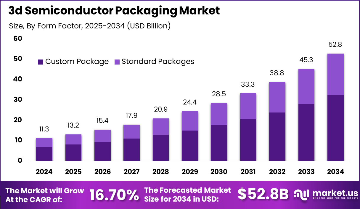
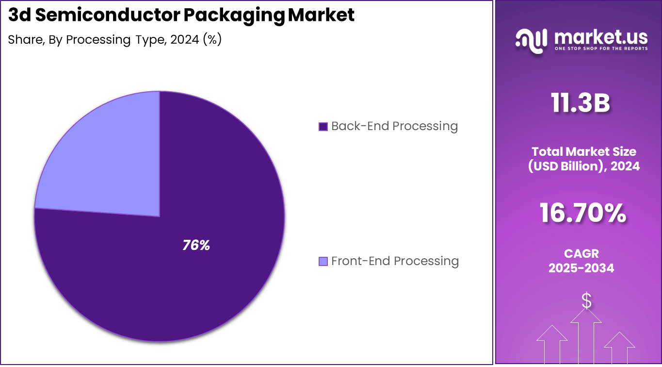
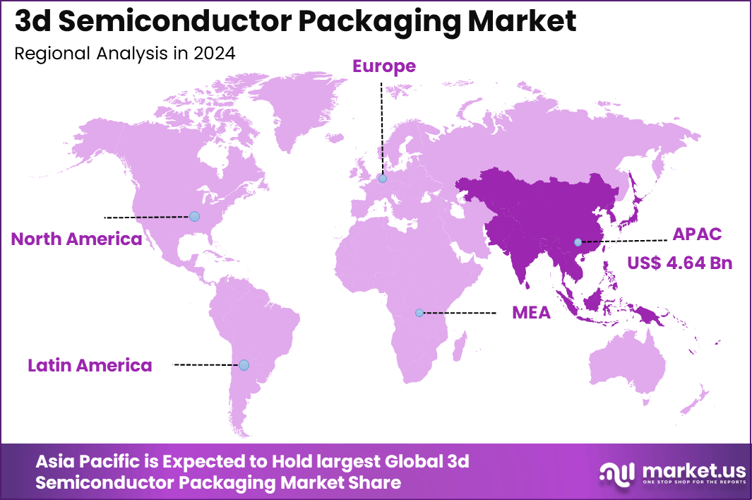
The Global 3d Semiconductor Packaging Market generated USD 11.3 billion in 2024 and is predicted to register growth from USD 13.2 billion in 2025 to about USD 52.8 billion by 2034, recording a CAGR of 16.70% throughout the forecast span. In 2024, Asia Pacific held a dominan market position, capturing more than a 41.2% share, holding USD 4.64 Billion revenue.
The 3D semiconductor packaging market has expanded as chip manufacturers adopt advanced stacking and integration techniques to meet rising performance needs. Growth reflects the shift from traditional planar packaging toward vertical architectures that support higher density, lower latency and improved power efficiency. The market benefits from increasing demand for compact, high performance chips across computing, mobile devices, automotive systems and industrial electronics.
The growth of the market can be attributed to rising demand for high bandwidth memory, growth in edge computing, and increasing adoption of AI and high performance workloads. Shrinking transistor scaling limits have encouraged the industry to shift toward 3D structures to maintain performance improvements. The need for reduced power consumption, better thermal performance and shorter interconnect pathways also supports wider adoption of 3D packaging.
Top Market Takeaways
- By technology, Through-Silicon Via (TSV) dominates with 35.8% share, valued for high-density vertical interconnections, superior electrical performance, and reduced latency. TSV is critical in 3D stacked memory, image sensors, and logic-memory integration used in AI and high-performance computing.
- By application, consumer electronics lead with 40.3% share, driven by demand for compact, high-performance semiconductors in smartphones, tablets, wearables, and consumer gadgets.
- By material type, organic substrates dominate at 52.4% share due to their flexibility, cost-effectiveness, and compatibility with high-volume manufacturing. They support advanced packaging designs like fan-out wafer-level packaging (FOWLP) and system-in-package (SiP).
- By end-user, electronics manufacturers represent 64.9% of the market as they integrate advanced 3D packaging to meet evolving performance and miniaturization demands.
- By form factor, custom packages lead with 61.6% share, reflecting increasing demand for tailored semiconductor solutions for specific applications across industries.
- By processing type, back-end processing dominates with 76.1% share, encompassing final assembly, testing, and packaging stages critical for 3D semiconductor devices reliability and performance.
By Technology
In 2024, Through-Silicon Via (TSV) technology holds a significant 35.8% share in the 3D semiconductor packaging market. TSV enables vertical electrical interconnections through silicon wafers, allowing multiple layers of chips to be stacked and interconnected directly. This reduces signal delay, power consumption, and heat generation, improving performance for compact, high-speed devices.
TSV’s ability to support dense vertical stacking makes it a critical technology for advanced computing, AI, and data center applications. The popularity of TSV comes from its benefits in reducing footprint while enhancing chip functionality. The technology is increasingly adopted to meet the demand for faster, smaller, and more efficient electronics, particularly in consumer devices and high-performance sectors. It supports a wide range of applications by offering better electrical integrity and reliability.
By Application
In 2024, Consumer electronics dominate the application segment with a 40.3% share. The ever-increasing demand for smaller, faster, and energy-efficient devices such as smartphones, tablets, wearables, and smart home technologies fuels the growth of 3D semiconductor packaging in this sector. These devices require high-density packaging solutions to accommodate complex chips while maintaining performance standards.
Advancements in 3D packaging enable manufacturers to deliver compact form factors and better thermal dissipation, which are crucial for enhancing device longevity and user experience. The constant innovation cycle and high consumer spending power continue to drive the adoption of 3D semiconductor technologies in consumer electronics.
By Material Type
In 2024, Organic substrates account for the majority share of 52.4% in material types used in 3D semiconductor packaging. These substrates, typically made from epoxy resins like FR-4 or BT resin, offer flexibility, light weight, and ease of processing compared to ceramics or metals. They support complex geometries, making them ideal for stacking multiple dies in various configurations.
The cost-effectiveness and good mechanical properties of organic substrates make them highly attractive for high-volume consumer electronics manufacturing. Their improved yield rates and reliability help meet performance demands while aligning with industry trends toward sustainability and efficiency in semiconductor production.
By End-User
In 2024, Electronics manufacturers are the dominant end-users, representing about 64.9% of the market. These companies leverage 3D semiconductor packaging to develop compact, high-performance products that meet modern consumer and industrial technology needs. Advanced packaging solutions help manufacturers optimize device performance, power efficiency, and form factors.
The large volume demand from consumer electronics, automotive, and industrial sectors drives investment in 3D packaging technologies. Electronics manufacturers increasingly focus on integrating 3D packaging to stay competitive by enhancing product design flexibility and reducing time to market.
By Form Factor
In 2024, Custom packages make up a substantial 61.6% of the form factor segment in 3D semiconductor packaging. Custom packaging allows electronics makers to tailor solutions specifically to device requirements, which is essential for differentiated products across consumer, automotive, and specialized industrial markets.
This flexibility supports unique stacking arrangements, die sizes, and interconnect designs that standard packages cannot accommodate. The preference for custom packages reflects the demand for optimized performance, space-saving integration, and innovation in device architecture.
By Processing Type
In 2024, Back-end processing dominates the market with approximately 76.1% share, reflecting its critical role in advanced semiconductor packaging. This phase involves assembling, testing, and finishing semiconductor devices after wafer fabrication, ensuring functional and reliable packages.
The increasing complexity of 3D packaging requires sophisticated back-end processes for precise die stacking, interconnect formation, and thermal management. Industry leaders are investing heavily in back-end technology to improve production efficiency and handle the demands of next-generation semiconductor products.
Key Market Segments
By Technology
- Through-Silicon Via (TSV)
- Micro-Bump Technology
- Wafer-Level Packaging (WLP)
- Fan-Out Packaging
By Application
- Consumer Electronics
- Automotive
- Telecommunications
- Industrial
By Material Type
- Silicon
- Organic Substrates
- Ceramics
By End-User
- Electronics Manufacturers
- Automotive Manufacturers
- Telecommunications Providers
- Industrial Equipment Manufacturers
By Form Factor
- Standard Packages
- Custom Package
By Processing Type
- Front-End Processing
- Back-End Processing
Emerging Trends
Key Trend Description Miniaturization Focus Rising demand for smaller, high-density semiconductor packages that support compact electronic devices and wearables is driving strong adoption of advanced packaging technologies. Heterogeneous Integration Integration of multiple chip types and technologies within a single package is enhancing performance, improving efficiency, and enabling multi-functionality in modern electronics. Advanced Interconnect Technologies Increasing use of TSVs, microbumps, and copper pillar bonding is enabling high-density vertical stacking and superior electrical performance in semiconductor packaging. AI and 5G Growth Influence Growing deployments of AI accelerators, 5G infrastructure, and high-performance computing systems are accelerating the demand for innovative packaging solutions. Sustainable Packaging Practices There is rising emphasis on eco-friendly materials and energy-efficient semiconductor manufacturing practices, supporting global sustainability objectives. Growth Factors
Key Factor Description Growing Need for High Performance Increasing demand for fast processing, low latency, and reduced power consumption in advanced electronics is reinforcing the adoption of next-generation packaging solutions. Expansion in Consumer Electronics Rising production of smartphones, wearables, and IoT devices is driving packaging innovation to support compactness, durability, and energy efficiency. Government and Industry Investments Significant R&D funding, infrastructure improvements, and regulatory support across major economies are accelerating semiconductor packaging advancements. Emerging Markets Growth Rapid industrialization and scaling electronics manufacturing in Asia-Pacific are strengthening the region’s role as a dominant market for semiconductor packaging. Technological Advancements in Packaging Continuous innovation in packaging materials, tools, and processes is improving performance efficiency while lowering production costs. Regional Analysis
Asia Pacific asserted its dominance in the 3D semiconductor packaging market, commanding a substantial 41.2% share. The region’s growth is chiefly driven by the presence of a robust semiconductor manufacturing base in countries including Taiwan, South Korea, Japan, and India, alongside China.
Accelerated adoption of cutting-edge packaging technologies such as heterogeneous integration, wafer-level packaging, and advanced thermal management drives this market forward. The surge in demand for consumer electronics, electric vehicles, and high-performance computing devices further fuels growth.
Supporting factors include strong government backing, noteworthy R&D investments, and a well-established supply chain that enhances the region’s competitiveness in delivering innovative and cost-effective packaging solutions.
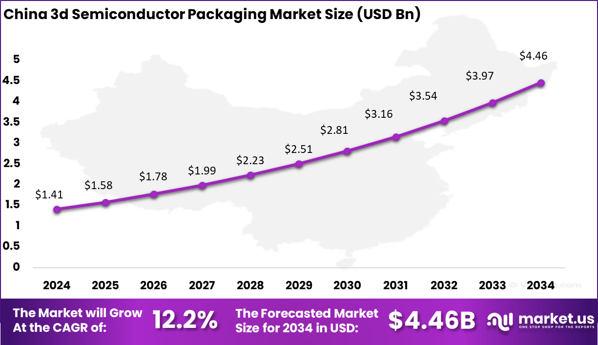
China stands out within Asia Pacific as a pivotal market, valued at approximately USD 1.41 billion in 2024, spearheading innovation and production in 3D semiconductor packaging. The country benefits from expansive foundry capacities, aggressive government initiatives aimed at semiconductor self-reliance, and a rapidly growing consumer electronics and automotive market.
Key Regions and Countries
- North America
- US
- Canada
- Europe
- Germany
- France
- The UK
- Spain
- Italy
- Russia
- Netherlands
- Rest of Europe
- Asia Pacific
- China
- Japan
- South Korea
- India
- Australia
- Singapore
- Thailand
- Vietnam
- Rest of APAC
- Latin America
- Brazil
- Mexico
- Rest of Latin America
- Middle East & Africa
- South Africa
- Saudi Arabia
- UAE
- Rest of MEA
Driver
Rising Demand for Miniaturized and High-Performance Electronics
The 3D semiconductor packaging market is largely driven by the growing demand for miniaturized, high-performance, and energy-efficient electronic devices. Technologies such as AI, IoT, 5G connectivity, and autonomous vehicles require powerful processing capabilities within compact footprints. 3D packaging allows stacking multiple chips vertically, reducing interconnection distances, enhancing speed, and improving power efficiency compared to traditional 2D packaging.
This miniaturization trend supports the development of smaller, smarter consumer electronics, data centers, and automotive systems. Increasing investments by semiconductor manufacturers in advanced packaging technologies and R&D fuel market growth, particularly in regions like Asia Pacific which dominate production.
Restraint
Technical Complexity and Thermal Management Challenges
Despite its potential, the 3D semiconductor packaging market faces considerable restraint from technical complexities, especially relating to thermal management and manufacturing precision. Stacking chips vertically creates densely packed structures generating significant heat that is difficult to dissipate effectively, risking performance degradation and reliability issues.
Additionally, processes like Through-Silicon Vias (TSV) and wafer-level packaging demand precise alignment and advanced bonding techniques, leading to lower yields and higher costs. These challenges hinder wider adoption and necessitate substantial investment in specialized equipment and expertise.
Opportunity
Growing Adoption in Automotive and Data Center Applications
There are abundant opportunities as demand surges in automotive electronics and data center markets. The automotive sector, particularly with ADAS and electric vehicles, needs sophisticated packaging for enhanced processing power and reliability under harsh conditions. Data centers require extensive high-performance computing resources with tight space and power constraints, which 3D packaging addresses.
Emerging applications in healthcare and industrial IoT further diversify use cases. Expanding integration with heterogeneous systems and novel materials offers pathways for innovation and new product development, providing substantial market potential.
Challenge
Rising Production Costs and Supply Chain Disruptions
A significant challenge is balancing the rising production costs with cost-effectiveness to meet diverse market needs. Advanced materials, equipment, and processes elevate manufacturing expenses, which can restrict adoption to high-value applications or large manufacturers.
Moreover, ongoing global supply chain disruptions affect the availability of raw materials and semiconductor components critical to packaging, causing delays and price volatility. Companies must enhance supply chain resilience and optimize manufacturing to sustain growth and competitiveness.
Competitive Analysis
Amkor Technology, ASE Group, TSMC, and Samsung Electronics lead the 3D semiconductor packaging market with strong capabilities in advanced packaging technologies such as 2.5D/3D IC, wafer-level packaging, and through-silicon via integration. Their solutions support high-performance computing, AI accelerators, and next-generation mobile devices. These companies focus on improving density, thermal efficiency, and power management.
Intel, Micron, Broadcom, GlobalFoundries, Infineon, NXP Semiconductors, ON Semiconductor, Renesas, STMicroelectronics, Texas Instruments, and Qualcomm strengthen the competitive landscape with diversified packaging portfolios. Their technologies enable faster data transfer, lower latency, and improved reliability for automotive electronics, industrial systems, and data-center workloads.
Jiangsu Changjiang Electronics Technology, Lattice Semiconductor, Marvell, SPIL, Sony, and other participants expand the market with cost-efficient, scalable packaging options for consumer electronics, communication devices, and edge-processing systems. Their focus is on flexible production, reduced manufacturing complexity, and optimized form factors.
Top Key Players in the Market
- Amkor Technology
- ASE Group (Advanced Semiconductor Engineering)
- Broadcom Inc.
- GlobalFoundries
- Infineon Technologies
- Intel Corporation
- Jiangsu Changjiang Electronics Technology Co.
- Lattice Semiconductor Corporation
- Marvell Technology Group
- Micron Technology
- NXP Semiconductors
- ON Semiconductor
- Qualcomm Incorporated
- Renesas Electronics Corporation
- Samsung Electronics
- Siliconware Precision Industries Co., Ltd. (SPIL)
- Sony Corporation
- STMicroelectronics
- Texas Instruments
- TSMC (Taiwan Semiconductor Manufacturing Company)
- Others
Future Outlook
The future outlook for the 3D semiconductor packaging market is highly promising, driven by increasing demand for miniaturization, higher performance, and energy efficiency in electronic devices. Key opportunities include advancements in heterogenous integration, improved thermal management solutions, and innovations in wafer-level packaging techniques.Aspect Description Heterogeneous Integration Growing adoption of integrated chip architectures combining multiple chip types within a single package enhances processing efficiency and device speed. Advanced Thermal Solutions Continuous innovation in heat-dissipation materials and structures supports better reliability and performance in dense semiconductor packages. Wafer-Level Packaging Increasing development of wafer-level and fan-out techniques is reducing manufacturing costs while improving package size and electrical performance. Application Growth Areas Demand is rising across AI, IoT, 5G, automotive electronics, and aerospace, where reliable, compact, and energy-efficient packaging is essential. Regional Growth Asia Pacific continues to lead global adoption driven by strong manufacturing capacity, while North America shows robust growth supported by innovation-focused ecosystems. Recent Developments
- November, 2025, Amkor announced plans to expand its chip manufacturing capacity in Korea with three new production lines and additional testing equipment at its Incheon plant. The company also highlighted its leadership in semiconductor packaging and AI integration at SEMICON West 2025
- August, 2025, ASE acquired WIN Semiconductors’ facility in Taiwan for NT$6.5 billion to expand advanced packaging capacity, targeting increased demand from AI and high-performance computing sectors. ASE expects its advanced packaging and testing revenues to grow significantly in 2025
Report Scope
Report Features Description Market Value (2024) USD 11.3 Bn Forecast Revenue (2034) USD 52.8 Bn CAGR(2025-2034) 16.70% Base Year for Estimation 2024 Historic Period 2020-2023 Forecast Period 2025-2034 Report Coverage Revenue forecast, AI impact on Market trends, Share Insights, Company ranking, competitive landscape, Recent Developments, Market Dynamics and Emerging Trends Segments Covered By Technology (Through-Silicon Via (TSV), Micro-Bump Technology, Wafer-Level Packaging (WLP), Fan-Out Packaging), By Application (Consumer Electronics, Automotive, Telecommunications, Industrial), By Material Type (Silicon, Organic Substrates, Ceramics), By End-User (Electronics Manufacturers, Automotive Manufacturers, Telecommunications Providers, Industrial Equipment Manufacturers), By Form Factor (Standard Packages, Custom Package), By Processing Type (Front-End Processing, Back-End Processing) Regional Analysis North America – US, Canada; Europe – Germany, France, The UK, Spain, Italy, Russia, Netherlands, Rest of Europe; Asia Pacific – China, Japan, South Korea, India, New Zealand, Singapore, Thailand, Vietnam, Rest of Latin America; Latin America – Brazil, Mexico, Rest of Latin America; Middle East & Africa – South Africa, Saudi Arabia, UAE, Rest of MEA Competitive Landscape Amkor Technology, ASE Group (Advanced Semiconductor Engineering), Broadcom Inc., GlobalFoundries, Infineon Technologies, Intel Corporation, Jiangsu Changjiang Electronics Technology Co., Lattice Semiconductor Corporation, Marvell Technology Group, Micron Technology, NXP Semiconductors, ON Semiconductor, Qualcomm Incorporated, Renesas Electronics Corporation, Samsung Electronics, Siliconware Precision Industries Co., Ltd. (SPIL), Sony Corporation, STMicroelectronics, Texas Instruments, TSMC (Taiwan Semiconductor Manufacturing Company), and others Customization Scope Customization for segments, region/country-level will be provided. Moreover, additional customization can be done based on the requirements. Purchase Options We have three license to opt for: Single User License, Multi-User License (Up to 5 Users), Corporate Use License (Unlimited User and Printable PDF)  3D Semiconductor Packaging MarketPublished date: Nov. 2025add_shopping_cartBuy Now get_appDownload Sample
 -
-
- Samsung Electronics Co Ltd.
- United Microelectronics Corporation
- Intel Corporation
- ACM Research
- Taiwan Semiconductor Manufacturing Company
- ASE Technology Holdings Co. Ltd.
- Amkor Technology
- Jiangsu Changjiang Electronics Technology Co. Ltd.
- Siliconware Precision Industries Co. Ltd. (SPIL)
- Powertech Technology Inc.
Our Clients
- 128640
- Nov. 2025